- 您现在的位置:买卖IC网 > PDF目录10688 > AD7823YRZ (Analog Devices Inc)IC ADC 8BIT SRL 2.7/5.5V 8-SOIC PDF资料下载
参数资料
| 型号: | AD7823YRZ |
| 厂商: | Analog Devices Inc |
| 文件页数: | 7/11页 |
| 文件大小: | 0K |
| 描述: | IC ADC 8BIT SRL 2.7/5.5V 8-SOIC |
| 标准包装: | 98 |
| 位数: | 8 |
| 采样率(每秒): | 200k |
| 数据接口: | 串行 |
| 转换器数目: | 1 |
| 功率耗散(最大): | 17.5mW |
| 电压电源: | 单电源 |
| 工作温度: | -40°C ~ 125°C |
| 安装类型: | 表面贴装 |
| 封装/外壳: | 8-SOIC(0.154",3.90mm 宽) |
| 供应商设备封装: | 8-SOIC |
| 包装: | 管件 |
| 输入数目和类型: | 2 个伪差分,单极 |
| 产品目录页面: | 779 (CN2011-ZH PDF) |
AD7823
–5–
REV. C
The AD7823 is tested using the CCIF standard where two input
frequencies near the top end of the input bandwidth are used.
In this case, the second and third order terms are of different
significance. The second order terms are usually distanced in
frequency from the original sine waves while the third order
terms are usually at a frequency close to the input frequencies.
As a result, the second and third order terms are specified sepa-
rately. The calculation of the intermodulation distortion is as
per the THD specification where it is the ratio of the rms sum of
the individual distortion products to the rms amplitude of the
fundamental expressed in dBs.
Relative Accuracy
Relative accuracy or endpoint nonlinearity is the maximum
deviation from a straight line passing through the endpoints of
the ADC transfer function.
Differential Nonlinearity
This is the difference between the measured and the ideal
1 LSB change between any two adjacent codes in the ADC.
Offset Error
This is the deviation of the first code transition (0000 . . . 000)
to (0000 . . . 001) from the ideal, i.e., AGND + 1 LSB.
Gain Error
This is the deviation of the last code transition (1111 . . . 110)
to (1111 . . . 111) from the ideal (i.e., VREF – 1 LSB) after the
offset error has been adjusted out.
Track/Hold Acquisition Time
Track/hold acquisition time is the time required for the output
of the track/hold amplifier to reach its final value, within
± 1/2 LSB, after the end of conversion (the point at which the
track/hold returns to track mode). It also applies to situations
where there is a step input change on the input voltage applied
to the VIN+ input of the AD7823. It means that the user must
wait for the duration of the track/hold acquisition time, after the
end of conversion or after a step input change to VIN, before
starting another conversion to ensure that the part operates to
specification.
TERMINOLOGY
Signal to (Noise + Distortion) Ratio
This is the measured ratio of signal to (noise + distortion) at the
output of the A/D converter. The signal is the rms amplitude of
the fundamental. Noise is the rms sum of all nonfundamental
signals up to half the sampling frequency (f
S/2), excluding dc.
The ratio is dependent upon the number of quantization levels
in the digitization process; the more levels, the smaller the
quantization noise. The theoretical signal to (noise + distortion)
ratio for an ideal N-bit converter with a sine wave input is
given by:
Signal to (Noise + Distortion) = (6.02N + 1.76) dB
Thus for an 8-bit converter, this is 50 dB.
Total Harmonic Distortion
Total harmonic distortion (THD) is the ratio of the rms sum of
harmonics to the fundamental. For the AD7823 it is defined as:
THD (dB)
= 20 log
V2
2 +V
3
2 +V
4
2 +V
5
2 +V
6
2
V1
where V1 is the rms amplitude of the fundamental and V2, V3,
V4, V5 and V6 are the rms amplitudes of the second through the
sixth harmonics.
Peak Harmonic or Spurious Noise
Peak harmonic or spurious noise is defined as the ratio of the
rms value of the next largest component in the ADC output
spectrum (up to fS/2 and excluding dc) to the rms value of
the fundamental. Normally, the value of this specification is
determined by the largest harmonic in the spectrum, but for
parts where the harmonics are buried in the noise floor, it
will be a noise peak.
Intermodulation Distortion
With inputs consisting of sine waves at two frequencies, fa and
fb, any active device with nonlinearities will create distortion
products at sum and difference frequencies of mfa
± nfb where
m, n = 0, 1, 2, 3, etc. Intermodulation terms are those for which
neither m nor n are equal to zero. For example, the second
order terms include (fa + fb) and (fa – fb), while the third order
terms include (2fa + fb), (2fa – fb), (fa + 2fb) and (fa – 2fb).
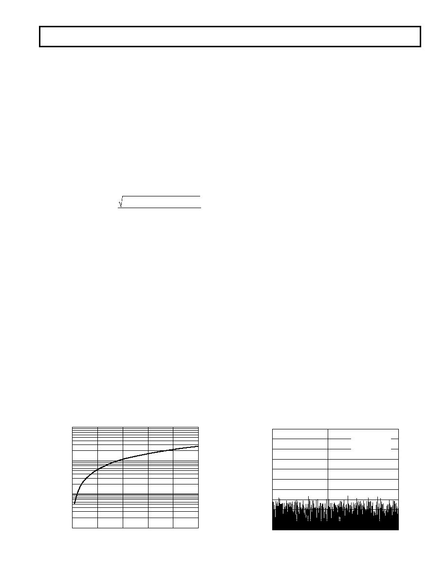
Typical Performance Characteristics
THROUGHPUT – kSPS
10
0
0.01
030
POWER
–
mW
10
0.1
20
40
50
Figure 2. Power vs. Throughput
FREQUENCY BINS
0
–70
–100
dBs
–10
–60
–80
–90
–30
–50
–20
–40
1
23
45
67
89
111
133
155
177
199
221
243
265
287
309
331
353
375
397
419
441
463
485
507
529
551
573
595
617
639
661
683
705
727
749
771
793
815
837
859
881
903
925
947
969
991
1013
AD7823
2048 POINT FFT
SAMPLING 136.054
fIN 29.961
Figure 3. AD7823 SNR
相关PDF资料 |
PDF描述 |
|---|---|
| LTC1540IMS8#TRPBF | IC COMP NANOPOWER W/REF 8-MSOP |
| ISL4489EIBZ | TRANSCEIVER RS-485/422 14-SOIC |
| LTC1540IMS8#TR | IC COMP 300NA 2% VOLT REF 8-MSOP |
| AD7819YRZ | IC ADC 8BIT SAMPLING PAR 16-SOIC |
| ISL4485EIBZ | IC TXRX RS-485/422 5V ESD 8-SOIC |
相关代理商/技术参数 |
参数描述 |
|---|---|
| AD7823YRZ-REEL | 功能描述:IC ADC 8BIT SRL 2.7-5.5V 8SOIC RoHS:是 类别:集成电路 (IC) >> 数据采集 - 模数转换器 系列:- 产品培训模块:Lead (SnPb) Finish for COTS Obsolescence Mitigation Program 标准包装:2,500 系列:- 位数:12 采样率(每秒):3M 数据接口:- 转换器数目:- 功率耗散(最大):- 电压电源:- 工作温度:- 安装类型:表面贴装 封装/外壳:SOT-23-6 供应商设备封装:SOT-23-6 包装:带卷 (TR) 输入数目和类型:- |
| AD7823YRZ-REEL7 | 功能描述:IC ADC 8BIT SRL 2.7-5.5V 8SOIC RoHS:是 类别:集成电路 (IC) >> 数据采集 - 模数转换器 系列:- 标准包装:2,500 系列:- 位数:16 采样率(每秒):15 数据接口:MICROWIRE?,串行,SPI? 转换器数目:1 功率耗散(最大):480µW 电压电源:单电源 工作温度:-40°C ~ 85°C 安装类型:表面贴装 封装/外壳:38-WFQFN 裸露焊盘 供应商设备封装:38-QFN(5x7) 包装:带卷 (TR) 输入数目和类型:16 个单端,双极;8 个差分,双极 配用:DC1011A-C-ND - BOARD DELTA SIGMA ADC LTC2494 |
| AD7824 | 制造商:AD 制造商全称:Analog Devices 功能描述:LC2MOS High Speed 4- & 8-Channel 8-Bit ADCs |
| AD7824BCHIPS | 制造商:未知厂家 制造商全称:未知厂家 功能描述:Single-Ended Data Acquisition System |
| AD7824BQ | 功能描述:IC ADC 8BIT LC2MOS 4CH HS 24CDIP RoHS:否 类别:集成电路 (IC) >> 数据采集 - 模数转换器 系列:- 其它有关文件:TSA1204 View All Specifications 标准包装:1 系列:- 位数:12 采样率(每秒):20M 数据接口:并联 转换器数目:2 功率耗散(最大):155mW 电压电源:模拟和数字 工作温度:-40°C ~ 85°C 安装类型:表面贴装 封装/外壳:48-TQFP 供应商设备封装:48-TQFP(7x7) 包装:Digi-Reel® 输入数目和类型:4 个单端,单极;2 个差分,单极 产品目录页面:1156 (CN2011-ZH PDF) 其它名称:497-5435-6 |
发布紧急采购,3分钟左右您将得到回复。