参数资料
| 型号: | AD7827BRZ |
| 厂商: | Analog Devices Inc |
| 文件页数: | 12/12页 |
| 文件大小: | 0K |
| 描述: | IC ADC 8BIT SAMPLING SRL 8SOIC |
| 产品变化通告: | AD7827 Series Discontinuation 18/Jul/2012 |
| 标准包装: | 98 |
| 位数: | 8 |
| 采样率(每秒): | 1M |
| 数据接口: | DSP,串行 |
| 转换器数目: | 1 |
| 功率耗散(最大): | 30mW |
| 电压电源: | 单电源 |
| 工作温度: | -40°C ~ 105°C |
| 安装类型: | 表面贴装 |
| 封装/外壳: | 8-SOIC(0.154",3.90mm 宽) |
| 供应商设备封装: | 8-SOIC |
| 包装: | 管件 |
| 输入数目和类型: | 1 个单端,单极 |
AD7827
–9–
REV. 0
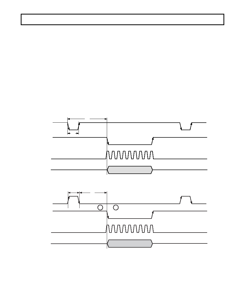
OPERATING MODES
The AD7827 has two possible modes of operation depending on
the state of the
CONVST pulse at the end of a conversion.
Mode 1 Operation (High Speed Sampling)
When the AD7827 is operated in Mode 1 the device is not
powered down between conversions. This mode of operation
allows high throughput rates to be achieved. Figure 13 shows
how this optimum throughput rate is achieved by bringing
CONVST high before the end of the conversion. When operat-
ing in this mode, a new conversion should not be initiated until
30 ns after the end of a read operation. This is to allow the
track/hold to acquire the analog signal to 0.5 LSB accuracy.
Mode 2 Operation (Automatic Power-Down)
When the AD7827 is operated in Mode 2 (see Figure 14) it
automatically powers down 530 ns after the falling edge of
CONVST. The CONVST signal is brought low to initiate a
conversion and is left logic low until 530 ns has elapsed after the
falling edge of the
CONVST pulse, i.e., before Point A or Point
B in Figure 14, depending on the actual value of t
2 (see Timing
Characteristics). The state of the
CONVST signal is sampled at
this point (i.e., 530 ns after
CONVST falling edge) and the
AD7827 will power down as long as the
CONVST is low. The
ADC is powered up again on the rising edge of the
CONVST
signal. The
CONVST pulse width does not have to be as long as
the power-up time if an external reference is used (see Power-Up
Times section). Superior power performance can be achieved in
this mode of operation by powering up the AD7827 to only
carry out a conversion. The serial interface of the AD7827 is
still fully operational while the device is powered down.
t2
t1
CURRENT CONVERSION
RESULT
CONVST
RFS
SCLK
DOUT
Figure 13. Mode 1 Operation Timing Diagram
t2
CURRENT CONVERSION
RESULT
CONVST
RFS
SCLK
DOUT
tPOWER-UP
A
B
Figure 14. Mode 2 Operation Timing Diagram
相关PDF资料 |
PDF描述 |
|---|---|
| AD7828LPZ-REEL | IC ADC 8BIT 8CH HS 28-PLCC |
| AD7829BRW-1 | IC ADC 8BIT 8CH 2MSPS 28-SOIC |
| AD7834BR | IC DAC 14BIT QUAD SRL 28-SOIC |
| AD7836ASZ | IC DAC 14BIT QUAD LC2MOS 44MQFP |
| AD7837BQ | IC DAC 12BIT DUAL MULT 24-CDIP |
相关代理商/技术参数 |
参数描述 |
|---|---|
| AD7827BRZ-REEL | 功能描述:IC ADC 8BIT SAMPLING SRL 8SOIC RoHS:是 类别:集成电路 (IC) >> 数据采集 - 模数转换器 系列:- 产品培训模块:Lead (SnPb) Finish for COTS Obsolescence Mitigation Program 标准包装:2,500 系列:- 位数:12 采样率(每秒):3M 数据接口:- 转换器数目:- 功率耗散(最大):- 电压电源:- 工作温度:- 安装类型:表面贴装 封装/外壳:SOT-23-6 供应商设备封装:SOT-23-6 包装:带卷 (TR) 输入数目和类型:- |
| AD7827BRZ-REEL7 | 功能描述:IC ADC 8BIT SAMPLING SRL 8SOIC RoHS:是 类别:集成电路 (IC) >> 数据采集 - 模数转换器 系列:- 产品培训模块:Lead (SnPb) Finish for COTS Obsolescence Mitigation Program 标准包装:2,500 系列:- 位数:12 采样率(每秒):3M 数据接口:- 转换器数目:- 功率耗散(最大):- 电压电源:- 工作温度:- 安装类型:表面贴装 封装/外壳:SOT-23-6 供应商设备封装:SOT-23-6 包装:带卷 (TR) 输入数目和类型:- |
| AD7828 | 制造商:AD 制造商全称:Analog Devices 功能描述:LC2MOS High Speed 4- & 8-Channel 8-Bit ADCs |
| AD7828BCHIPS | 制造商:未知厂家 制造商全称:未知厂家 功能描述:Single-Ended Data Acquisition System |
| AD7828BQ | 功能描述:IC ADC 8BIT 8CH HS 28-CDIP RoHS:否 类别:集成电路 (IC) >> 数据采集 - 模数转换器 系列:- 标准包装:1 系列:- 位数:14 采样率(每秒):83k 数据接口:串行,并联 转换器数目:1 功率耗散(最大):95mW 电压电源:双 ± 工作温度:0°C ~ 70°C 安装类型:通孔 封装/外壳:28-DIP(0.600",15.24mm) 供应商设备封装:28-PDIP 包装:管件 输入数目和类型:1 个单端,双极 |
发布紧急采购,3分钟左右您将得到回复。