参数资料
| 型号: | AD7834AN |
| 厂商: | Analog Devices Inc |
| 文件页数: | 16/28页 |
| 文件大小: | 0K |
| 描述: | IC DAC 14BIT QUAD SRL 28-DIP |
| 产品培训模块: | Data Converter Fundamentals DAC Architectures |
| 标准包装: | 13 |
| 设置时间: | 10µs |
| 位数: | 14 |
| 数据接口: | 串行 |
| 转换器数目: | 4 |
| 电压电源: | 模拟和数字,双 ± |
| 功率耗散(最大): | 465mW |
| 工作温度: | -40°C ~ 85°C |
| 安装类型: | 通孔 |
| 封装/外壳: | 28-DIP(0.600",15.24mm) |
| 供应商设备封装: | 28-PDIP |
| 包装: | 管件 |
| 输出数目和类型: | 4 电压,单极;4 电压,双极 |
| 采样率(每秒): | 100k |
第1页第2页第3页第4页第5页第6页第7页第8页第9页第10页第11页第12页第13页第14页第15页当前第16页第17页第18页第19页第20页第21页第22页第23页第24页第25页第26页第27页第28页
AD7834/AD7835
Rev. D | Page 23 of 28
APPLICATIONS INFORMATION
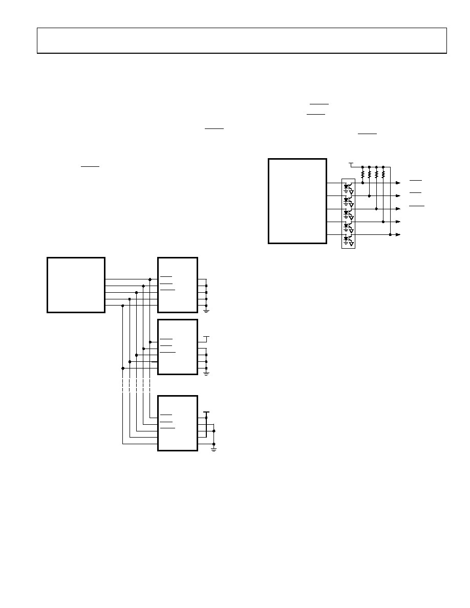
Figure 34 shows a 5-channel isolated interface to the AD7834.
Multiple devices are connected to the outputs of the opto-coupler
and controlled as for serial interfacing. To reduce the number of
opto-isolators, the
SERIAL INTERFACE TO MULTIPLE AD7834S
Figure 33 shows how the package address pins of the AD7834
are used to address multiple AD7834s. This figure shows only
10 devices, but up to 32 AD7834s can each be assigned a unique
address by hardwiring each of the package address pins to VCC
or DGND. Normal operation of the device occurs when
PAEN line doesn’t need to be controlled if it
is not used. If the PAEN line is not controlled by the microcon-
troller, it should be tied low at each device. If simultaneous updat-
ing of the DACs is not required, the
PAEN
is low. When serial data is being written to the AD7834s, only
the device with the same package address as the package address
contained in the serial data accepts data into the input registers.
Conversely, if
LDAC pin on each part can
be tied permanently low and another opto-isolator is not needed.
MICROCONTROLLER
CONTROL OUT
SYNC OUT
SERIAL CLOCK OUT
SERIAL DATA OUT
OPTO-COUPLER
VCC
TO PAENs
TO LDACs
TO FSYNCs
TO SCLKs
TO DINs
01
00
6-
03
4
PAEN is high, the package address is ignored, and
the data is loaded into the same channel on each package.
The primary limitation with multiple packages is the output
update rate. For example, if an output update rate of 10 kHz is
required, 100 μs are available to load all DACs. Assuming a
serial clock frequency of 10 MHz, it takes 2.5 μs to load data to
one DAC. Thus, 40 DACs or 10 packages can be updated in this
time. As the update rate requirement decreases, the number of
possible packages increases.
1ADDITIONAL PINS OMITTED FOR CLARITY
AD78341
DEVICE 0
PAEN
LDAC
FSYNC
SCLK
DIN
PA0
PA1
PA2
PA3
PA4
VCC
MICROCONTROLLER
CONTROL OUT
SYNC OUT
SERIAL CLOCK OUT
SERIAL DATA OUT
AD78341
DEVICE 1
PAEN
LDAC
FSYNC
SCLK
DIN
PA0
PA1
PA2
PA3
PA4
AD78341
DEVICE 9
PAEN
LDAC
FSYNC
SCLK
DIN
PA0
PA1
PA2
PA3
PA4
01
00
6-
03
3
Figure 34. Opto-Isolated Interface
AUTOMATED TEST EQUIPMENT
The AD7834/AD7835 are particularly suited for use in an
automated test environment. Figure 35 shows the AD7835
providing the necessary voltages for the pin driver and the
window comparator in a typical ATE pin electronics configur-
ation. Two AD588s are used to provide reference voltages for
the AD7835. In the configuration shown, the AD588s are
configured so that the voltage at Pin 1 is 5 V greater than the
voltage at Pin 9 and the voltage at Pin 15 is 5 V less than the
voltage at Pin 9.
One
is used as a reference for DAC 1 and DAC 2. These
DACs are used to provide high and low levels for the pin driver.
The pin driver can have an associated offset. This can be nulled
by applying an offset voltage to Pin 9 of the AD588. First, the
code 1000 . . . 0000 is loaded into the DAC 1 latch, and the pin
driver output is set to the DAC 1 output. The VOFFSET voltage is
adjusted until 0 V appears between the pin driver output and
DUT GND. This causes both VREF(+)A and VREF()A to be off-
set with respect to AGND by an amount equal to VOFFSET.
However, the output of the pin driver varies from 5 V to +5 V
with respect to DUT GND as the DAC input code varies from
000 . . . 000 to 111 . . . 111. The VOFFSET voltage is also applied to
the DSGA pin. When a clear is performed on the AD7835, the
output of the pin driver is 0 V with respect to DUT GND.
Figure 33. Serial Interface to Multiple AD7834s
OPTO-ISOLATED INTERFACE
In many process control applications, it is necessary to provide
an isolation barrier between the controller and the unit being
controlled. Opto-isolators can provide voltage isolation in
excess of 3 kV. The serial loading structure of the AD7834
makes it ideal for opto-isolated interfaces because the number
of interface lines is kept to a minimum.
相关PDF资料 |
PDF描述 |
|---|---|
| VE-B6M-MU-S | CONVERTER MOD DC/DC 10V 200W |
| VE-B6H-MU-S | CONVERTER MOD DC/DC 52V 200W |
| VI-BNF-MU-S | CONVERTER MOD DC/DC 72V 200W |
| VI-BND-MU-S | CONVERTER MOD DC/DC 85V 200W |
| VE-B6D-MU-S | CONVERTER MOD DC/DC 85V 200W |
相关代理商/技术参数 |
参数描述 |
|---|---|
| AD7834ANZ | 功能描述:IC DAC 14BIT QUAD SRL 28-DIP RoHS:是 类别:集成电路 (IC) >> 数据采集 - 数模转换器 系列:- 标准包装:1 系列:- 设置时间:4.5µs 位数:12 数据接口:串行,SPI? 转换器数目:1 电压电源:单电源 功率耗散(最大):- 工作温度:-40°C ~ 125°C 安装类型:表面贴装 封装/外壳:8-SOIC(0.154",3.90mm 宽) 供应商设备封装:8-SOICN 包装:剪切带 (CT) 输出数目和类型:1 电压,单极;1 电压,双极 采样率(每秒):* 其它名称:MCP4921T-E/SNCTMCP4921T-E/SNRCTMCP4921T-E/SNRCT-ND |
| AD7834AR | 功能描述:IC DAC 14BIT QUAD SRL 28-SOIC RoHS:否 类别:集成电路 (IC) >> 数据采集 - 数模转换器 系列:- 产品培训模块:Lead (SnPb) Finish for COTS Obsolescence Mitigation Program 标准包装:1,000 系列:- 设置时间:1µs 位数:8 数据接口:串行 转换器数目:8 电压电源:双 ± 功率耗散(最大):941mW 工作温度:0°C ~ 70°C 安装类型:表面贴装 封装/外壳:24-SOIC(0.295",7.50mm 宽) 供应商设备封装:24-SOIC W 包装:带卷 (TR) 输出数目和类型:8 电压,单极 采样率(每秒):* |
| AD7834AR-REEL | 功能描述:IC DAC 14BIT QUAD SRL 28-SOIC RoHS:否 类别:集成电路 (IC) >> 数据采集 - 数模转换器 系列:- 标准包装:2,400 系列:- 设置时间:- 位数:18 数据接口:串行 转换器数目:3 电压电源:模拟和数字 功率耗散(最大):- 工作温度:-40°C ~ 85°C 安装类型:表面贴装 封装/外壳:36-TFBGA 供应商设备封装:36-TFBGA 包装:带卷 (TR) 输出数目和类型:* 采样率(每秒):* |
| AD7834ARZ | 功能描述:IC DAC 14BIT QUAD SRL 28-SOIC RoHS:是 类别:集成电路 (IC) >> 数据采集 - 数模转换器 系列:- 标准包装:1 系列:- 设置时间:4.5µs 位数:12 数据接口:串行,SPI? 转换器数目:1 电压电源:单电源 功率耗散(最大):- 工作温度:-40°C ~ 125°C 安装类型:表面贴装 封装/外壳:8-SOIC(0.154",3.90mm 宽) 供应商设备封装:8-SOICN 包装:剪切带 (CT) 输出数目和类型:1 电压,单极;1 电压,双极 采样率(每秒):* 其它名称:MCP4921T-E/SNCTMCP4921T-E/SNRCTMCP4921T-E/SNRCT-ND |
| AD7834ARZ-REEL | 功能描述:IC DAC 14BIT QUAD SERIAL 28SOIC RoHS:是 类别:集成电路 (IC) >> 数据采集 - 数模转换器 系列:- 产品培训模块:Data Converter Fundamentals DAC Architectures 标准包装:750 系列:- 设置时间:7µs 位数:16 数据接口:并联 转换器数目:1 电压电源:双 ± 功率耗散(最大):100mW 工作温度:0°C ~ 70°C 安装类型:表面贴装 封装/外壳:28-LCC(J 形引线) 供应商设备封装:28-PLCC(11.51x11.51) 包装:带卷 (TR) 输出数目和类型:1 电压,单极;1 电压,双极 采样率(每秒):143k |
发布紧急采购,3分钟左右您将得到回复。