参数资料
| 型号: | AD7840KPZ |
| 厂商: | Analog Devices Inc |
| 文件页数: | 14/16页 |
| 文件大小: | 0K |
| 描述: | IC DAC 14BIT LOW PWR 5V 28-PLCC |
| 产品培训模块: | Data Converter Fundamentals DAC Architectures |
| 标准包装: | 1 |
| 设置时间: | 2.5µs |
| 位数: | 14 |
| 数据接口: | 串行,并联 |
| 转换器数目: | 1 |
| 电压电源: | 双 ± |
| 功率耗散(最大): | 100mW |
| 工作温度: | 0°C ~ 70°C |
| 安装类型: | 表面贴装 |
| 封装/外壳: | 28-LCC(J 形引线) |
| 供应商设备封装: | 28-PLCC(11.51x11.51) |
| 包装: | 管件 |
| 输出数目和类型: | 1 电压,双极 |
| 采样率(每秒): | 400k |
AD7840
REV. B
–7–
Table III. Parallel Mode Truth Table
CS
WR
LDAC
Function
HX
H
}Both Latches Latched
XH
H
L
H
Input Latch Transparent
HH
L
}
Input Latch Latched
H
X
L
DAC Latch Transparent
X
H
L
Analog Output Updated
ff
L
Input Latch Transparent
DAC Latch Data Transfer Inhibited
L
g
L
}Input Latch Is Latched
g
L
DAC Latch Data Transfer Occurs
X = Don’t Care
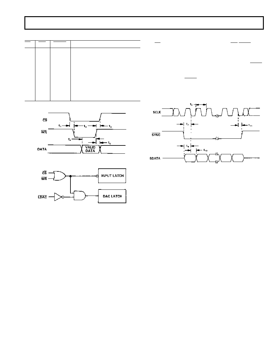
Figure 6. Parallel Mode Timing Diagram
Figure 7. AD7840 Simplified Parallel Input Control Logic
Serial Data Format
The serial data format is selected for the AD7840 by connecting
the CS/SERIAL line to –5 V. In this case, the WR/SYNC,
D13/SDATA, D12/SCLK, D11/FORMAT and D10/JUSTIFY
pins all assume their serial functions. The unused parallel inputs
should not be left unconnected to avoid noise pickup. Serial
data is loaded to the input latch under control of SCLK, SYNC
and SDATA. The AD7840 expects a 16-bit stream of serial data
on its SDATA input. Serial data must be valid on the falling
edge of SCLK. The SYNC input provides the frame synchroni-
zation signal which tells the AD7840 that valid serial data will
be available for the next 16 falling edges of SCLK. Figure 8
shows the timing diagram for serial data format.
Figure 8. Serial Mode Timing Diagram
Although 16 bits of data are clocked into the AD7840, only 14
bits go into the input latch. Therefore, two bits in the stream are
don’t cares since their value does not affect the input latch data.
The order and position in which the AD7840 accepts the 14 bits
of input data depends upon the FORMAT and JUSTIFY in-
puts. There are four different input data modes which can be
chosen (see Table I in the Pin Function Description section).
The first mode (M1) assumes that the first two bits of the input
data stream are don’t cares, the third bit is the LSB and the last
(or 16th bit) is the MSB. This mode is chosen by tying both the
FORMAT and JUSTIFY pins to a logic 0. The second mode
(M2; FORMAT = 0, JUSTIFY = 1) assumes that the first bit in
the data stream is the LSB, the fourteenth bit is the MSB and
the last two bits are don’t cares. The third mode (M3;
FORMAT= 1, JUSTIFY 0) assumes that the first two bits in
the stream are again don’t cares, the third bit is now the MSB
and the sixteenth bit is the LSB. The final mode (M4; FOR-
MAT = 1, JUSTIFY= 1) assumes that the first bit is the MSB,
the fourteenth bit is the LSB and the last two bits of the stream
are don’t cares.
相关PDF资料 |
PDF描述 |
|---|---|
| VI-B63-MY-B1 | CONVERTER MOD DC/DC 24V 50W |
| VI-B62-MY-B1 | CONVERTER MOD DC/DC 15V 50W |
| VI-2WK-IV-F3 | CONVERTER MOD DC/DC 40V 150W |
| VI-B4X-MY-B1 | CONVERTER MOD DC/DC 5.2V 50W |
| VI-B4W-MY-B1 | CONVERTER MOD DC/DC 5.5V 50W |
相关代理商/技术参数 |
参数描述 |
|---|---|
| AD7840KPZ-RL | 功能描述:14 Bit Digital to Analog Converter 1 28-PLCC (11.51x11.51) 制造商:analog devices inc. 系列:- 包装:带卷(TR) 零件状态:在售 位数:14 数模转换器数:1 建立时间:4μs 输出类型:Voltage - Buffered 差分输出:无 数据接口:并联,串行 参考类型:外部, 内部 电压 - 电源,模拟:±5V 电压 - 电源,数字:- INL/DNL(LSB):±1(最大),±0.9(最大) 架构:R-2R 工作温度:0°C ~ 70°C 封装/外壳:28-LCC(J 形引线) 供应商器件封装:28-PLCC(11.51x11.51) 标准包装:1 |
| AD7840LN | 制造商:未知厂家 制造商全称:未知厂家 功能描述:14-Bit Digital-to-Analog Converter |
| AD7840LP | 制造商:未知厂家 制造商全称:未知厂家 功能描述:14-Bit Digital-to-Analog Converter |
| AD7840SE/883B | 制造商:未知厂家 制造商全称:未知厂家 功能描述:14-Bit Digital-to-Analog Converter |
| AD7840SQ | 制造商:AD 制造商全称:Analog Devices 功能描述:LC2MOS Complete 14-Bit DAC |
发布紧急采购,3分钟左右您将得到回复。