- 您现在的位置:买卖IC网 > PDF目录8562 > AD7841ASZ-REEL (Analog Devices Inc)IC DAC 14BIT OCTAL VOUT 44-MQFP PDF资料下载
参数资料
| 型号: | AD7841ASZ-REEL |
| 厂商: | Analog Devices Inc |
| 文件页数: | 13/13页 |
| 文件大小: | 0K |
| 描述: | IC DAC 14BIT OCTAL VOUT 44-MQFP |
| 产品培训模块: | Data Converter Fundamentals DAC Architectures |
| 标准包装: | 800 |
| 设置时间: | 31µs |
| 位数: | 14 |
| 数据接口: | 并联 |
| 转换器数目: | 8 |
| 电压电源: | 模拟和数字,双 ± |
| 功率耗散(最大): | 303mW |
| 工作温度: | -40°C ~ 85°C |
| 安装类型: | 表面贴装 |
| 封装/外壳: | 44-QFP |
| 供应商设备封装: | 44-MQFP(10x10) |
| 包装: | 带卷 (TR) |
| 输出数目和类型: | 8 电压,单极;8 电压,双极 |
| 采样率(每秒): | 32k |
| 配用: | EVAL-AD7841EBZ-ND - BOARD EVAL FOR AD7841 |
AD7841
–9–
Power-On with
CLR Low
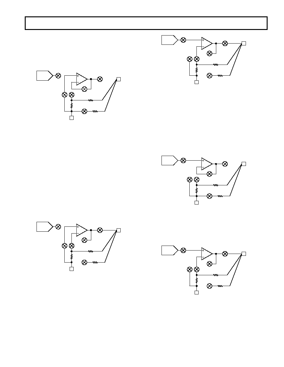
The output stage of the AD7841 has been designed to allow
output stability during power-on. If
CLR is kept low during
power-on, then just after power is applied to the AD7841, the
situation is as depicted in Figure 5. G1, G4 and G6 are open
while G2, G3 and G5 are closed.
G1
G2
G4
G3
G6
G5
DUTGND
VOUT
R
14k
DAC
Figure 5. Output Stage with VDD < 7 V or VSS > –3 V; CLR
Low
VOUT is kept within a few hundred millivolts of DUTGND via
G5 and a 14 k
resistor. This thin-film resistor is connected in
parallel with the gain resistors of the output amplifier. The
output amplifier is connected as a unity gain buffer via G3, and
the DUTGND voltage is applied to the buffer input via G2. The
amplifier’s output is thus at the same voltage as the DUTGND
pin. The output stage remains configured as in Figure 5 until
the voltage at VDD exceeds 7 V and VSS is more negative than
–3 V. By now the output amplifier has enough headroom to
handle signals at its input and has also had time to settle. The
internal power-on circuitry opens G3 and G5 and closes G4 and
G6. This situation is shown in Figure 6. Now the output ampli-
fier is configured in its noise gain configuration via G4 and G6.
The DUTGND voltage is still connected to the noninverting
input via G2 and this voltage appears at VOUT.
G1
G2
G4
G3
G6
G5
DUTGND
VOUT
R
14k
DAC
Figure 6. Output Stage with VDD > 7 V and VSS < –3 V; CLR
Low
VOUT has been disconnected from the DUTGND pin by the
opening of G5, but will track the voltage present at DUTGND
via the configuration shown in Figure 6.
When
CLR is taken back high, the output stage is configured as
shown in Figure 7. The internal control logic closes G1 and
opens G2. The output amr})fier is connected in a noninverting
gain-of-two configuration. The voltage that appears on the VOUT
pins is determined by the data present in the DAC registers.
G1
G2
G4
G3
G6
G5
DUTGND
VOUT
R
14k
DAC
Figure 7. Output Stage After
CLR Is Taken High
Power-On with
CLR High
If
CLR is high on the application of power to the device, the
output stages of the AD7841 are configured as in Figure 8 while
VDD is less than 7 V and VSS is more positive than –3 V. G1 is
closed and G2 is open, thereby connecting the output of the
DAC to the input of its output amplifier. G3 and G5 are closed
while G4 and G6 are open, thus connecting the output amplifier as
a unity gain buffer. VOUT is connected to DUTGND via G5
through a 14 k
resistor until V
DD exceeds 7 V and VSS is more
negative than –3 V.
G1
G2
G4
G3
G6
G5
DUTGND
VOUT
R
14k
DAC
Figure 8. Output Stage Powering Up with
CLR High
While VDD < 7 V or VSS > –3 V
When the difference between the supply voltages reaches 10 V,
the internal power-on circuitry opens G3 and G5 and closes G4
and G6 configuring the output stage as shown in Figure 9.
G1
G2
G4
G3
G6
G5
DUTGND
VOUT
R
14k
DAC
Figure 9. Output Stage Powering Up with
CLR High
When VDD > 7 V and VSS < –3 V
REV. B
相关PDF资料 |
PDF描述 |
|---|---|
| VE-J1X-MZ-B1 | CONVERTER MINIMOD DC/DC 5.2V 25W |
| VI-BNR-MU-S | CONVERTER MOD DC/DC 7.5V 200W |
| MAX4090EXT+T | IC VIDEO BUFFER 6DB SC70-6 |
| MAX9509ATA+T | IC AMP VIDEO FILTER 8-TDFN |
| VE-BWP-MX-S | CONVERTER MOD DC/DC 13.8V 75W |
相关代理商/技术参数 |
参数描述 |
|---|---|
| AD7841BS | 制造商:Analog Devices 功能描述:DAC 8-CH R-2R 14-bit 44-Pin MQFP 制造商:Rochester Electronics LLC 功能描述:OCTAL 14 BIT HIGH VOLTAGE IC - Bulk 制造商:Analog Devices 功能描述:Digital-Analog Converter IC Interface Ty |
| AD7841BS-REEL | 制造商:Analog Devices 功能描述:DAC 8-CH R-2R 14-bit 44-Pin MQFP T/R 制造商:Analog Devices 功能描述:DAC 8CH R-2R 14BIT 44MQFP - Tape and Reel |
| AD7841BSZ | 功能描述:IC DAC 14BIT OCTAL V-OUT 44-MQFP RoHS:是 类别:集成电路 (IC) >> 数据采集 - 数模转换器 系列:- 产品培训模块:Lead (SnPb) Finish for COTS Obsolescence Mitigation Program 标准包装:50 系列:- 设置时间:4µs 位数:12 数据接口:串行 转换器数目:2 电压电源:单电源 功率耗散(最大):- 工作温度:-40°C ~ 85°C 安装类型:表面贴装 封装/外壳:8-TSSOP,8-MSOP(0.118",3.00mm 宽) 供应商设备封装:8-uMAX 包装:管件 输出数目和类型:2 电压,单极 采样率(每秒):* 产品目录页面:1398 (CN2011-ZH PDF) |
| AD7841BSZ | 制造商:Analog Devices 功能描述:IC 14-BIT DAC |
| AD7841BSZ-REEL | 功能描述:IC DAC 14BIT OCTAL VOUT 44-MQFP RoHS:是 类别:集成电路 (IC) >> 数据采集 - 数模转换器 系列:- 产品培训模块:Lead (SnPb) Finish for COTS Obsolescence Mitigation Program 标准包装:1,000 系列:- 设置时间:1µs 位数:8 数据接口:串行 转换器数目:8 电压电源:双 ± 功率耗散(最大):941mW 工作温度:0°C ~ 70°C 安装类型:表面贴装 封装/外壳:24-SOIC(0.295",7.50mm 宽) 供应商设备封装:24-SOIC W 包装:带卷 (TR) 输出数目和类型:8 电压,单极 采样率(每秒):* |
发布紧急采购,3分钟左右您将得到回复。