- 您现在的位置:买卖IC网 > PDF目录165343 > AD7845KRZ (ANALOG DEVICES INC) PARALLEL, WORD INPUT LOADING, 2.5 us SETTLING TIME, 12-BIT DAC, PDSO24 PDF资料下载
参数资料
| 型号: | AD7845KRZ |
| 厂商: | ANALOG DEVICES INC |
| 元件分类: | DAC |
| 英文描述: | PARALLEL, WORD INPUT LOADING, 2.5 us SETTLING TIME, 12-BIT DAC, PDSO24 |
| 封装: | SOIC-24 |
| 文件页数: | 5/12页 |
| 文件大小: | 196K |
| 代理商: | AD7845KRZ |
(VDD = +15 V,
5%, VSS = –15 V,
5%, VREF = +10 V, AGND = DGND = O V,
VOUT connected to RFB. VOUT load = 2 k , 100 pF. All specifications TMIN to TMAX unless otherwise noted.)
REV. B
–2–
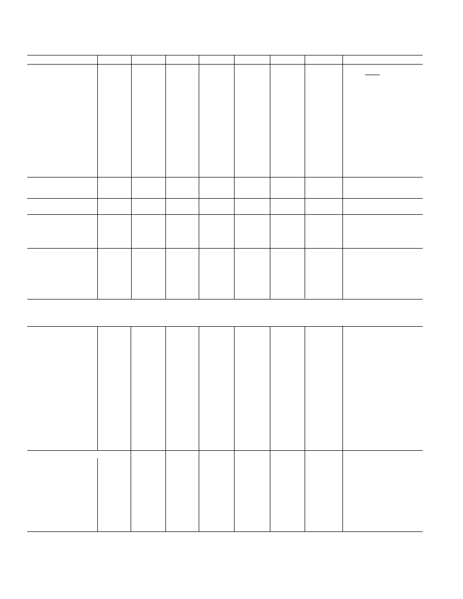
AD7845–SPECIFICATIONS1
Parameter
J Version
K Version
A Version
B Version
S Version
T Version
Units
Test Conditions/Comments
ACCURACY
Resolution
12
Bits
1 LSB =
V
REF
212
= 2.4 mV
Relative Accuracy
at +25
°C
±1
±1/2
±1
±1/2
±1
±1/2
LSB max
All Grades Are Guaranteed
TMIN to TMAX
±1
±3/4
±1
±3/4
±1
±3/4
LSB max
Monotonic over Temperature
Differential Nonlinearity
±1
LSB max
DAC Register Loaded with
Zero Code Offset Error
All 0s.
at +25
°C
±2
±1
±2
±1
±2
±1mV max
TMIN to TMAX
±3
±2
±3
±2
±4
±3mV max
Offset Temperature Coefficient;
(
Offset/Temperature)2
±5
V/°C typ
Gain Error
±3
±2
±3
±2
±3
±2
LSB max
RFB, VOUT Connected
±6
LSB max
RC, VOUT Connected, VREF = +5 V
±6
LSB max
RB, VOUT Connected, VREF = +5 V
±7
LSB max
RA, VOUT Connected, VREF = +2.5 V
Gain Temperature Coefficient;
(
Gain/Temperature)2
±2
ppm of FSR/
°CR
FB, VOUT Connected
typ
REFERENCE INPUT
Input Resistance, Pin 17
8888
88
k
min
Typical Input Resistance = 12 k
16
k
max
APPLICATION RESISTOR
RATIO MATCHING
0.5
0 5
% max
Matching Between RA, RB, RC
DIGITAL INPUTS
VIH (Input High Voltage)
2.4
V min
VIL (Input Low Voltage)
0.8
V max
IIN (Input Current)
±1
A max
Digital Inputs at 0 V and VDD
CIN (Input Capacitance)
2
7777
77
pF max
POWER SUPPLY
4
VDD Range
14.25/15.75
V min/V max
VSS Range
–14.25/–15.75 –14.25/–15.75 –14.25/–15.75 –14.25/–15.75
–14.25/–15.75 –14.25/–15.75
V min/V max
Power Supply Rejection
Gain/V
DD
±0.01
% per % max
VDD = +15 V
± 5%, V
REF = –10 V
Gain/V
SS
±0.01
% per % max
VSS = –15 V
± 5%.
IDD
6666
66
mA max
VOUT Unloaded
ISS
4444
44
mA max
VOUT Unloaded
AC PERFORMANCE CHARACTERISTICS
These characteristics are included for Design Guidance and are not subject to test.
DYNAMIC PERFORMANCE
Output Voltage Settling Time
5555
55
s max
To 0.01% of Full-Scale Range
V
OUT Load = 2 k, 100 pF.
DAC Register Alternately Loaded
with All 0s and All 1s. Typically
2.5
s at 25°C.
Slew Rate
11
V/
s typ
V
OUT Load = 2 k, 100 pF.
Digital-to-Analog
55
nV–s typ
Measured with V
REF = 0 V.
Glitch Impulse
DAC Register Alternately Loaded
with All 0s and All 1s.
Multiplying Feedthrough
5555
55
mV p-p typ
V
REF = ± 10 V, 10 kHz Sine Wave
Error3
DAC Register Loaded with All 0s.
Unity Gain Small Signal
Bandwidth
600
kHz typ
V
OUT, RFB Connected. DAC Loaded
with All 1s V
REF = 100 mV p-p
Sine Wave.
Full Power Bandwidth
175
kHz typ
V
OUT, RFB Connected. DAC Loaded
with All 1s. V
REF = 20 V p-p
Sine Wave. R
L = 2 k.
Total Harmonic Distortion
–90
dB typ
V
REF = 6 V rms, 1 kHz Sine Wave.
OUTPUT CHARACTERISTICS5
Open Loop Gain
85
dB min
VOUT, RFB Not Connected
VOUT =
±10 V, R
L = 2 k
Output Voltage Swing
±10
V min
RL = 2 k
, C
L = 100 pF
Output Resistance
0.2
typ
RFB, VOUT Connected,
Short Circuit Current @ +25
°C
11
mA typ
VOUT Shorted to AGND
Output Noise Voltage
Includes Noise Due to Output
(0.1 Hz to 10 Hz) @ +25
°C
2222
22
V rms typ
Amplifier and Johnson Noise
f = 10 Hz
250
nV/
√Hz typ
of RFB
f = 100 Hz
100
nV/
√Hz typ
f = 1 kHz
50
nV/
√Hz typ
f = 10 kHz
50
nV/
√Hz typ
f = 100 kHz
50
nV/
√Hz typ
NOTES
1Temperature ranges are as follows: J, K Versions: 0
°C to +70°C; A, B Versions: –40°C to +85°C; S, T Versions: –55°C to +125°C.
2Guaranteed by design and characterization, not production tested.
3The metal lid on the ceramic D-24A package is connected to Pin 12 (DGND).
4The device is functional with a power supply of
± 12 V.
5Minimum specified load resistance is 2 k
.
Specifications subject to change without notice.
相关PDF资料 |
PDF描述 |
|---|---|
| AD7911ARMZ-REEL | 2-CH 10-BIT SUCCESSIVE APPROXIMATION ADC, SERIAL ACCESS, PDSO8 |
| AD7911AUJZ-R2 | 2-CH 10-BIT SUCCESSIVE APPROXIMATION ADC, SERIAL ACCESS, PDSO8 |
| AD9551BCPZ | 900 MHz, OTHER CLOCK GENERATOR, QCC40 |
| AD9643BCPZ-170 | 2-CH 14-BIT FLASH METHOD ADC, PARALLEL ACCESS, QCC64 |
| AD9643BCPZ-210 | 2-CH 14-BIT FLASH METHOD ADC, PARALLEL ACCESS, QCC64 |
相关代理商/技术参数 |
参数描述 |
|---|---|
| AD7845KRZ-REEL | 功能描述:IC DAC 12BIT MULT LC2MOS 24-SOIC RoHS:是 类别:集成电路 (IC) >> 数据采集 - 数模转换器 系列:- 标准包装:47 系列:- 设置时间:2µs 位数:14 数据接口:并联 转换器数目:1 电压电源:单电源 功率耗散(最大):55µW 工作温度:-40°C ~ 85°C 安装类型:表面贴装 封装/外壳:28-SSOP(0.209",5.30mm 宽) 供应商设备封装:28-SSOP 包装:管件 输出数目和类型:1 电流,单极;1 电流,双极 采样率(每秒):* |
| AD7845SE | 制造商:AD 制造商全称:Analog Devices 功能描述:LC2MOS Complete 12-Bit Multiplying DAC |
| AD7845SE/883B | 功能描述:数模转换器- DAC COMPLETE 12 BIT MDAC IC RoHS:否 制造商:Texas Instruments 转换器数量:1 DAC 输出端数量:1 转换速率:2 MSPs 分辨率:16 bit 接口类型:QSPI, SPI, Serial (3-Wire, Microwire) 稳定时间:1 us 最大工作温度:+ 85 C 安装风格:SMD/SMT 封装 / 箱体:SOIC-14 封装:Tube |
| AD7845SE883B | 制造商:AD 制造商全称:Analog Devices 功能描述:LC2MOS Complete 12-Bit Multiplying DAC |
| AD7845SQ | 功能描述:数模转换器- DAC 12-BIT CMOS DAC IC RoHS:否 制造商:Texas Instruments 转换器数量:1 DAC 输出端数量:1 转换速率:2 MSPs 分辨率:16 bit 接口类型:QSPI, SPI, Serial (3-Wire, Microwire) 稳定时间:1 us 最大工作温度:+ 85 C 安装风格:SMD/SMT 封装 / 箱体:SOIC-14 封装:Tube |
发布紧急采购,3分钟左右您将得到回复。