参数资料
| 型号: | AD7846AP |
| 厂商: | Analog Devices Inc |
| 文件页数: | 6/24页 |
| 文件大小: | 0K |
| 描述: | IC DAC 16BIT LC2MOS VOUT 28PLCC |
| 产品培训模块: | Data Converter Fundamentals DAC Architectures |
| 标准包装: | 1 |
| 设置时间: | 7µs |
| 位数: | 16 |
| 数据接口: | 并联 |
| 转换器数目: | 1 |
| 电压电源: | 双 ± |
| 功率耗散(最大): | 100mW |
| 工作温度: | -40°C ~ 85°C |
| 安装类型: | 表面贴装 |
| 封装/外壳: | 28-LCC(J 形引线) |
| 供应商设备封装: | 28-PLCC(11.51x11.51) |
| 包装: | 管件 |
| 输出数目和类型: | 1 电压,单极;1 电压,双极 |
| 采样率(每秒): | 143k |
AD7846
Rev. G | Page 14 of 24
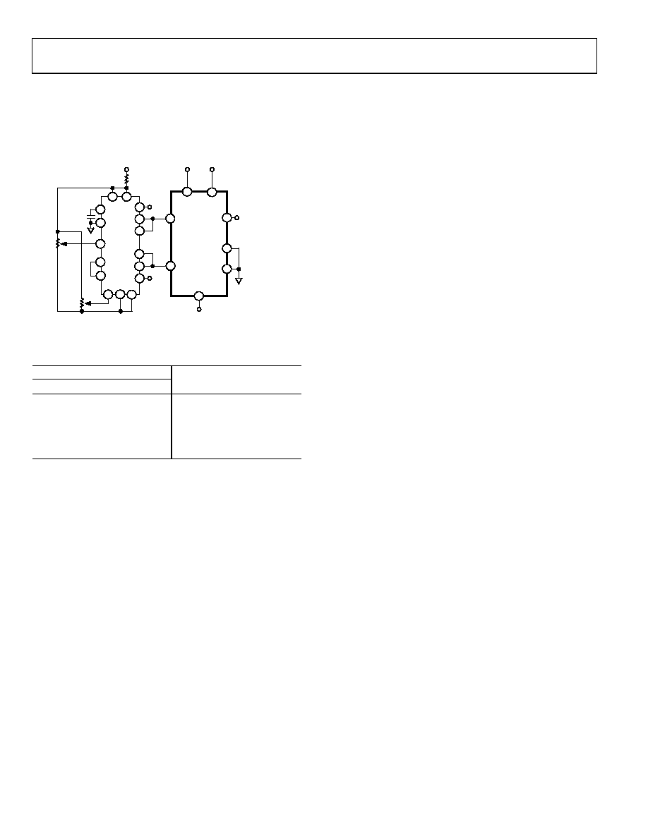
BIPOLAR OPERATION
Figure 24 shows the AD7846 set up for ±10 V bipolar operation.
The AD588 provides precision ±5 V tracking outputs that are
fed to the VREF+ and VREF inputs of the AD7846. The code table
DGND
+15V
+5V
VDD
VSS
VCC
VOUT
RIN
VREF+
VREF–
R2
10k
C1
1F
SIGNAL
GROUND
–15V
*ADDITIONAL PINS OMITTED FOR CLARITY
AD7846*
AD588
VOUT
(–10V TO +10V)
+15V
–15V
R3
100k
R1
39k
+15V
4
21
9
5
6
20
7
2
3
1
14
15
16
13
8
12
11
10
5
9
7
46
8
0
84
90
-0
24
Figure 24. Bipolar ±10 V Operation
Table 9. Offset Binary Code Table for Figure 24
Binary Number in DAC Latch
MSB
LSB1
Analog Output (VOUT)
1111 1111 1111 1111
+10 (32,767/32,768) V
1000 0000 0000 0001
+10 (1/32,768) V
1000 0000 0000 0000
0 V
0111 1111 1111 1111
10 (1/32,768) V
0000 0000 0000 0000
10 (32,768/32,768) V
1 LSB = 10 V/215 = 10 V/32,768 = 305 μV.
Full-scale and bipolar zero adjustment are provided by varying
the gain and balance on the AD588. R2 varies the gain on the
AD588 while R3 adjusts the +5 V and 5 V outputs together
with respect to ground.
For bipolar zero adjustment on the AD7846, load the DAC with
100…000 and adjust R3 until VOUT = 0 V. Full scale is adjusted
by loading the DAC with all 1s and adjusting R2 until VOUT =
9.999694 V.
When bipolar zero and full-scale adjustment are not needed, R2
and R3 can be omitted, Pin 12 on the AD588 should be connected
to Pin 11, and Pin 5 should be left floating. If a user wants a 5 V
output range, there are two choices. By tying Pin 6 (RIN) of the
AD7846 to VOUT (Pin 5), the output stage gain is reduced to
unity and the output range is ±5 V. If only a positive 5 V reference
is available, bipolar ±5 V operation is still possible. Tie VREF to
0 V and connect RIN to VREF+. This also gives a ±5 V output
range. However, the linearity, gain, and offset error specifications
are the same as the unipolar 0 V to 5 V range.
MULTIPLYING OPERATION
The AD7846 is a full multiplying DAC. To obtain four-quadrant
multiplication, tie VREF to 0 V, apply the ac input to VREF+, and
response when the DAC is used in this fashion.
相关PDF资料 |
PDF描述 |
|---|---|
| AD664JNZ-BIP | IC DAC 12BIT QUAD BIPOLAR 28-DIP |
| VI-B4N-MU-S | CONVERTER MOD DC/DC 18.5V 200W |
| VI-B44-MU-S | CONVERTER MOD DC/DC 48V 200W |
| VI-B13-MU-S | CONVERTER MOD DC/DC 24V 200W |
| VE-B4B-MU-S | CONVERTER MOD DC/DC 95V 200W |
相关代理商/技术参数 |
参数描述 |
|---|---|
| AD7846APZ | 功能描述:IC DAC 16BIT LC2MOS VOUT 28-PLCC RoHS:是 类别:集成电路 (IC) >> 数据采集 - 数模转换器 系列:- 产品培训模块:Lead (SnPb) Finish for COTS Obsolescence Mitigation Program 标准包装:1,000 系列:- 设置时间:1µs 位数:8 数据接口:串行 转换器数目:8 电压电源:双 ± 功率耗散(最大):941mW 工作温度:0°C ~ 70°C 安装类型:表面贴装 封装/外壳:24-SOIC(0.295",7.50mm 宽) 供应商设备封装:24-SOIC W 包装:带卷 (TR) 输出数目和类型:8 电压,单极 采样率(每秒):* |
| AD7846AQ | 制造商:Rochester Electronics LLC 功能描述: 制造商:Analog Devices 功能描述:IC,D/A CONVERTER,SINGLE,16-BIT,BICMOS,DIP,28PIN |
| AD7846BP | 功能描述:IC DAC 16BIT LC2MOS VOUT 28PLCC RoHS:否 类别:集成电路 (IC) >> 数据采集 - 数模转换器 系列:- 产品培训模块:Lead (SnPb) Finish for COTS Obsolescence Mitigation Program 标准包装:1,000 系列:- 设置时间:1µs 位数:8 数据接口:串行 转换器数目:8 电压电源:双 ± 功率耗散(最大):941mW 工作温度:0°C ~ 70°C 安装类型:表面贴装 封装/外壳:24-SOIC(0.295",7.50mm 宽) 供应商设备封装:24-SOIC W 包装:带卷 (TR) 输出数目和类型:8 电压,单极 采样率(每秒):* |
| AD7846BPZ | 功能描述:IC DAC 16BIT LC2MOS VOUT 28PLCC RoHS:是 类别:集成电路 (IC) >> 数据采集 - 数模转换器 系列:- 标准包装:1 系列:- 设置时间:4.5µs 位数:12 数据接口:串行,SPI? 转换器数目:1 电压电源:单电源 功率耗散(最大):- 工作温度:-40°C ~ 125°C 安装类型:表面贴装 封装/外壳:8-SOIC(0.154",3.90mm 宽) 供应商设备封装:8-SOICN 包装:剪切带 (CT) 输出数目和类型:1 电压,单极;1 电压,双极 采样率(每秒):* 其它名称:MCP4921T-E/SNCTMCP4921T-E/SNRCTMCP4921T-E/SNRCT-ND |
| AD7846BQ | 制造商:未知厂家 制造商全称:未知厂家 功能描述:16-Bit Digital-to-Analog Converter |
发布紧急采购,3分钟左右您将得到回复。