参数资料
| 型号: | AD7846KP |
| 厂商: | Analog Devices Inc |
| 文件页数: | 10/24页 |
| 文件大小: | 0K |
| 描述: | IC DAC 16BIT LC2MOS VOUT 28PLCC |
| 产品培训模块: | Data Converter Fundamentals DAC Architectures |
| 标准包装: | 1 |
| 设置时间: | 7µs |
| 位数: | 16 |
| 数据接口: | 并联 |
| 转换器数目: | 1 |
| 电压电源: | 双 ± |
| 功率耗散(最大): | 100mW |
| 工作温度: | 0°C ~ 70°C |
| 安装类型: | 表面贴装 |
| 封装/外壳: | 28-LCC(J 形引线) |
| 供应商设备封装: | 28-PLCC(11.51x11.51) |
| 包装: | 管件 |
| 输出数目和类型: | 1 电压,单极;1 电压,双极 |
| 采样率(每秒): | 143k |
AD7846
Rev. G | Page 18 of 24
APPLICATION HINTS
NOISE
In high resolution systems, noise is often the limiting factor.
With a 10 V span, a 16-bit LSB is 152 μV (–96 dB). Thus, the
noise floor must stay below 96 dB in the frequency range of
interest. Figure 12 shows the noise spectral density for the
AD7846.
GROUNDING
As well as noise, the other prime consideration in high resolution
DAC systems is grounding. With an LSB size of 152 μV and a
load current of 5 mA, 1 LSB of error can be introduced by series
resistance of only 0.03 Ω.
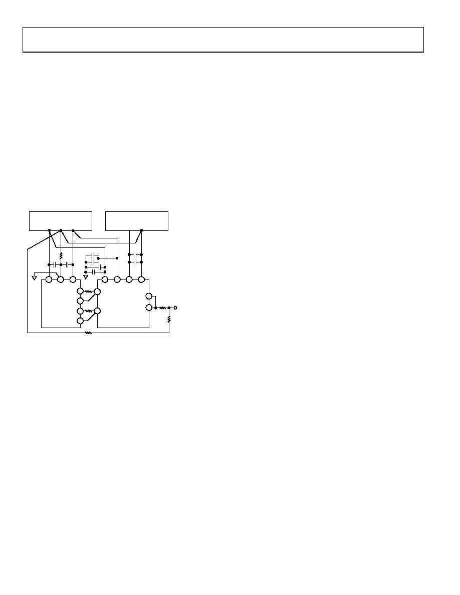
Figure 30 shows recommended grounding for the AD7846 in a
typical application.
ANALOG SUPPLY
DIGITAL SUPPLY
–15V
+15V 0V
DGND
+5V
SIGNAL
GROUND
AD7846*
AD588*
R1
R4
RL
VOUT
(+5V TO –5V)
R2
R3
R5
*ADDITIONAL PINS OMITTED FOR CLARITY
2
9
16
4
9
21
20
6
5
1
3
7
8
15
14
0
8490-
032
Figure 30. AD7846 Grounding
R1 to R5 represent lead and track resistances on the printed
circuit board. R1 is the resistance between the analog power
supply ground and the signal ground. Because current flowing
in R1 is very low (bias current of AD588 sense amplifier), the
effect of R1 is negligible. R2 and R3 represent track resistance
between the AD588 outputs and the AD7846 reference inputs.
Because of the force and sense outputs on the AD588, these
resistances will also have a negligible effect on accuracy.
R4 is the resistance between the DAC output and the load. If RL
is constant, then R4 introduces a gain error only that can be
trimmed out in the calibration cycle. R5 is the resistance
between the load and the analog common. If the output voltage
is sensed across the load, R5 introduces a further gain error,
which can be trimmed out. If, on the other hand, the output
voltage is sensed at the analog supply common, R5 appears as
part of the load and therefore introduces no errors.
PRINTED CIRCUIT BOARD LAYOUT
Figure 31 shows the AD7846 in a typical application with the
AD588 reference, producing an output analog voltage in the
±10 V range. Full-scale and bipolar zero adjustment are
provided by Potentiometer R2 and Potentiometer R3. Latches
(2 × 74LS245) isolate the DAC digital inputs from the active
microprocessor bus and minimize digital feedthrough.
相关PDF资料 |
PDF描述 |
|---|---|
| VI-B7P-MX-S | CONVERTER MOD DC/DC 13.8V 75W |
| AD5381BSTZ-3-REEL | IC DAC 12BIT 40CH 3V 100-LQFP |
| VI-B7N-MX-S | CONVERTER MOD DC/DC 18.5V 75W |
| VI-B7M-MX-S | CONVERTER MOD DC/DC 10V 75W |
| VI-B7L-MX-S | CONVERTER MOD DC/DC 28V 75W |
相关代理商/技术参数 |
参数描述 |
|---|---|
| AD7846KP-REEL | 制造商:AD 制造商全称:Analog Devices 功能描述:LC2MOS 16-Bit Voltage Output DAC |
| AD7846KPZ | 功能描述:IC DAC 16BIT LC2MOS VOUT 28PLCC RoHS:是 类别:集成电路 (IC) >> 数据采集 - 数模转换器 系列:- 标准包装:1 系列:- 设置时间:4.5µs 位数:12 数据接口:串行,SPI? 转换器数目:1 电压电源:单电源 功率耗散(最大):- 工作温度:-40°C ~ 125°C 安装类型:表面贴装 封装/外壳:8-SOIC(0.154",3.90mm 宽) 供应商设备封装:8-SOICN 包装:剪切带 (CT) 输出数目和类型:1 电压,单极;1 电压,双极 采样率(每秒):* 其它名称:MCP4921T-E/SNCTMCP4921T-E/SNRCTMCP4921T-E/SNRCT-ND |
| AD7846KPZ-REEL | 功能描述:IC DAC 16BIT LC2MOS VOUT 28PLCC RoHS:是 类别:集成电路 (IC) >> 数据采集 - 数模转换器 系列:- 产品培训模块:Lead (SnPb) Finish for COTS Obsolescence Mitigation Program 标准包装:1,000 系列:- 设置时间:1µs 位数:8 数据接口:串行 转换器数目:8 电压电源:双 ± 功率耗散(最大):941mW 工作温度:0°C ~ 70°C 安装类型:表面贴装 封装/外壳:24-SOIC(0.295",7.50mm 宽) 供应商设备封装:24-SOIC W 包装:带卷 (TR) 输出数目和类型:8 电压,单极 采样率(每秒):* |
| AD7846SD/883B | 制造商:未知厂家 制造商全称:未知厂家 功能描述:16-Bit Digital-to-Analog Converter |
| AD7846SE/883B | 制造商:未知厂家 制造商全称:未知厂家 功能描述:16-Bit Digital-to-Analog Converter |
发布紧急采购,3分钟左右您将得到回复。