参数资料
| 型号: | AD7849ANZ |
| 厂商: | Analog Devices Inc |
| 文件页数: | 7/20页 |
| 文件大小: | 0K |
| 描述: | IC DAC 16BIT SERIAL INP 20DIP |
| 产品培训模块: | Data Converter Fundamentals DAC Architectures |
| 标准包装: | 18 |
| 设置时间: | 7µs |
| 位数: | 14 |
| 数据接口: | 串行 |
| 转换器数目: | 1 |
| 电压电源: | 模拟和数字,双 ± |
| 功率耗散(最大): | 100mW |
| 工作温度: | -40°C ~ 85°C |
| 安装类型: | 通孔 |
| 封装/外壳: | 20-DIP(0.300",7.62mm) |
| 供应商设备封装: | 20-PDIP |
| 包装: | 管件 |
| 输出数目和类型: | 1 电压,单极;1 电压,双极 |
| 采样率(每秒): | 143k |
AD7849
Rev. C | Page 15 of 20
Other Output Voltage Ranges
In some cases, users may require output voltage ranges other than
those already mentioned. One example is systems that need the
output voltage to be a whole number of millivolts (that is,1 mV or
2 mV). If the circuit shown in Figure 22 is used, then the LSB size is
125 μV. This makes it possible to program whole millivolt values at
the output. Table 9 shows the code table for the circuit shown in
VDD
VCC
VREF+
VOUT
(0V TO 8.192V)
DGND
VREF–
AD7849*
AD584
SIGNAL
GND
1
*ADDITIONAL PINS OMITTED FOR CLARITY.
8
4
ROFS
AGND
R2
R1 8.192V
+15V
+5V
010
08-
023
Figure 22. 0 V to 8.192 V Output Range
Table 9. Code Table for Figure 22
Binary Number in DAC Latch
MSB
LSB
Analog Output (VOUT)
1111 1111 1111 1111
8.192 V (65,535/65,536) = 8.1919 V
1000 0000 0000 0000
8.192 V (32,768/65,536) = 4.096 V
0000 0000 0000 1000
8.192 V (8/65,536) = 0.001 V
0000 0000 0000 0100
8.192 V (4/65,536) = 0.0005 V
0000 0000 0000 0010
8.192 V (2/65,536) = 0.00025 V
0000 0000 0000 0001
8.192 V (1/65,536) = 0.000125 V
Generating a ±5 V Output Range from a Single +5 V
Reference
Figure 23 shows how to generate a ±5 V output range when
using a single +5 V reference. VREF is connected to 0 V, and ROFS
is connected to VREF+. The 5 V reference input is applied to these
pins. With all 0s loaded to the DAC, the noninverting terminal
of the output stage amplifier is at 0 V, and VOUT is the inverse of
VREF+. With all 1s loaded to the DAC, the noninverting terminal of
the output stage amplifier is 5 V and, therefore, VOUT is also 5 V.
ROFS
VDD
VCC
VREF+
VOUT
(–5V TO +5V)
DGND
VREF–
VSS
–15V
AD7849*
R1
10k
AD586
C1
1nF
SIGNAL GND
6
8
4
5
*ADDITIONAL PINS OMITTED FOR CLARITY.
2
AGND
+15V
+5V
01
00
8-
02
4
Figure 23. Generating a ±5 V Output Range from a Single +5 V
MICROPROCESSOR INTERFACING
Microprocessor interfacing to the AD7849 is via a serial bus
that uses standard protocol compatible with DSP processors
and microcontrollers. The communications channel requires a
3-wire interface consisting of a clock signal, a data signal, and a
synchronization signal. The AD7849 requires a 16-bit data-word
with data valid on the falling edge of SCLK. For all the interfaces,
the DAC update can be done automatically when all data is
clocked in, or it can be done under control of LDAC.
interfacing to a number of popular DSP processors and
microcontrollers.
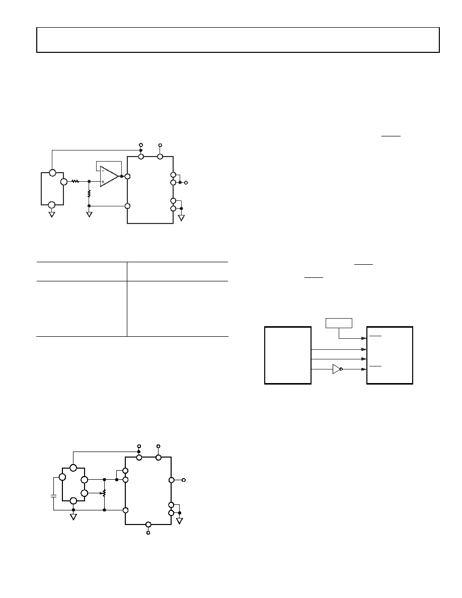
AD7849-to-DSP56000 Interface
A serial interface between the AD7849 and the DSP56000 is
shown in Figure 24. The DSP56000 is configured for normal
mode asynchronous operation with a gated clock. It is also
setup for a 16-bit word with SCK and SC2 as outputs and the
FSL control bit set to 0. SCK is internally generated on the
DSP56000 and applied to the AD7849 SCLK input. Data from
the DSP56000 is valid on the falling edge of SCK. The SC2 output
provides the framing pulse for valid data. This line must be
inverted before being applied to the SYNC input of the
.
In this interface, an LDAC pulse generated from an external timer
is used to update the outputs of the DAC. This update can also
be produced using a bit programmable control line from the
DSP56000.
DSP56000
SCK
STD
SC2
AD7849*
LDAC
SCLK
SDIN
SYNC
*ADDITIONAL PINS OMITTED FOR CLARITY.
TIMER
01008-029
Figure 24. AD7849-to-DSP56000 Interface
相关PDF资料 |
PDF描述 |
|---|---|
| VE-2T3-IV-F2 | CONVERTER MOD DC/DC 24V 150W |
| LTC1650ACS#TRPBF | IC D/A CONV 16BIT R-R 16-SOIC |
| VE-2T2-IV-F1 | CONVERTER MOD DC/DC 15V 150W |
| LTC1650ACS#TR | IC DAC 16BIT R-R VOLT OUT 16SOIC |
| VE-2T1-IV-F1 | CONVERTER MOD DC/DC 12V 150W |
相关代理商/技术参数 |
参数描述 |
|---|---|
| AD7849AR | 功能描述:IC DAC 16BIT SRL INP 20-SOIC RoHS:否 类别:集成电路 (IC) >> 数据采集 - 数模转换器 系列:- 产品培训模块:Data Converter Fundamentals DAC Architectures 标准包装:750 系列:- 设置时间:7µs 位数:16 数据接口:并联 转换器数目:1 电压电源:双 ± 功率耗散(最大):100mW 工作温度:0°C ~ 70°C 安装类型:表面贴装 封装/外壳:28-LCC(J 形引线) 供应商设备封装:28-PLCC(11.51x11.51) 包装:带卷 (TR) 输出数目和类型:1 电压,单极;1 电压,双极 采样率(每秒):143k |
| AD7849AR-REEL | 功能描述:IC DAC 16BIT SRL INP 20-SOIC RoHS:否 类别:集成电路 (IC) >> 数据采集 - 数模转换器 系列:- 标准包装:2,400 系列:- 设置时间:- 位数:18 数据接口:串行 转换器数目:3 电压电源:模拟和数字 功率耗散(最大):- 工作温度:-40°C ~ 85°C 安装类型:表面贴装 封装/外壳:36-TFBGA 供应商设备封装:36-TFBGA 包装:带卷 (TR) 输出数目和类型:* 采样率(每秒):* |
| AD7849ARZ | 功能描述:IC DAC 14/16BIT SRL-IN 20-SOIC RoHS:是 类别:集成电路 (IC) >> 数据采集 - 数模转换器 系列:- 标准包装:1 系列:- 设置时间:4.5µs 位数:12 数据接口:串行,SPI? 转换器数目:1 电压电源:单电源 功率耗散(最大):- 工作温度:-40°C ~ 125°C 安装类型:表面贴装 封装/外壳:8-SOIC(0.154",3.90mm 宽) 供应商设备封装:8-SOICN 包装:剪切带 (CT) 输出数目和类型:1 电压,单极;1 电压,双极 采样率(每秒):* 其它名称:MCP4921T-E/SNCTMCP4921T-E/SNRCTMCP4921T-E/SNRCT-ND |
| AD7849ARZ-REEL | 功能描述:IC DAC 14/16BIT SRL-IN 20-SOIC RoHS:是 类别:集成电路 (IC) >> 数据采集 - 数模转换器 系列:- 标准包装:47 系列:- 设置时间:2µs 位数:14 数据接口:并联 转换器数目:1 电压电源:单电源 功率耗散(最大):55µW 工作温度:-40°C ~ 85°C 安装类型:表面贴装 封装/外壳:28-SSOP(0.209",5.30mm 宽) 供应商设备封装:28-SSOP 包装:管件 输出数目和类型:1 电流,单极;1 电流,双极 采样率(每秒):* |
| AD7849BN | 制造商:Analog Devices 功能描述:DAC 1-CH R-2R 16-bit 20-Pin PDIP N Tube 制造商:Rochester Electronics LLC 功能描述:SERIAL INPUT,16-BIT DAC I.C. - Bulk |
发布紧急采购,3分钟左右您将得到回复。