参数资料
| 型号: | AD7849CNZ |
| 厂商: | Analog Devices Inc |
| 文件页数: | 6/20页 |
| 文件大小: | 0K |
| 描述: | IC DAC 16BIT SERIAL INP 20DIP |
| 产品培训模块: | Data Converter Fundamentals DAC Architectures |
| 标准包装: | 18 |
| 设置时间: | 7µs |
| 位数: | 16 |
| 数据接口: | 串行 |
| 转换器数目: | 1 |
| 电压电源: | 模拟和数字,双 ± |
| 功率耗散(最大): | 100mW |
| 工作温度: | -40°C ~ 85°C |
| 安装类型: | 通孔 |
| 封装/外壳: | 20-DIP(0.300",7.62mm) |
| 供应商设备封装: | 20-PDIP |
| 包装: | 管件 |
| 输出数目和类型: | 1 电压,单极;1 电压,双极 |
| 采样率(每秒): | 143k |
AD7849
Rev. C | Page 14 of 20
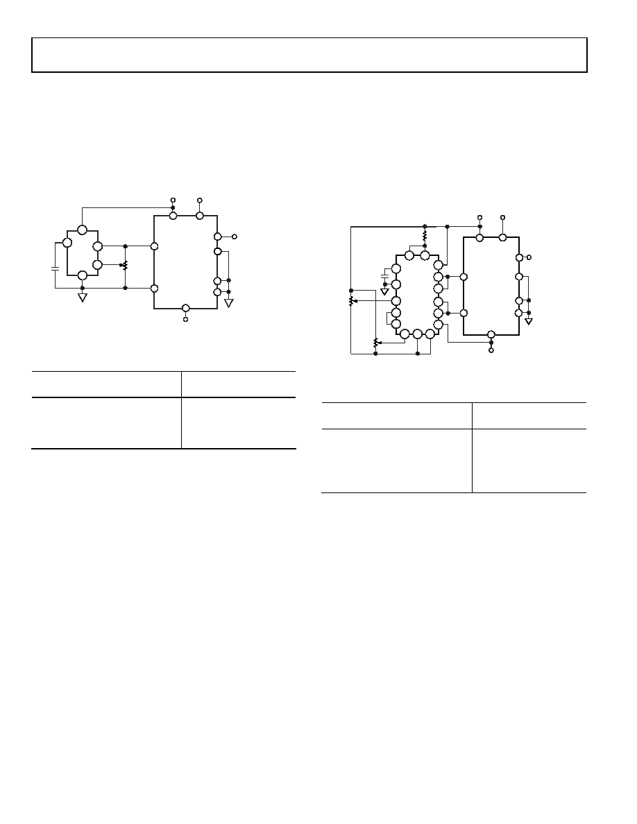
Unipolar Configuration
configuration. The DAC is driven by the AD586, 5 V reference.
Because ROFS is tied to 0 V, the output amplifier has a gain of ×2,
and the output range is 0 V to 10 V. If a 0 V to 5 V range is
required, ROFS should be tied to VOUT, configuring the output
stage for a gain of ×1. Table 7 gives the code table for the circuit
shown in Figure 20.
ROFS
VDD
VCC
VREF+
VOUT
(0V TO 10V)
AGND
VREF–
VSS
–15V
AD7849*
R1
10k
AD586
C1
1nF
SIGNAL GND
6
8
4
5
*ADDITIONAL PINS OMITTED FOR CLARITY.
2
DGND
+15V
+5V
01
00
8-
02
1
Figure 20. Unipolar Binary Operation
Table 7. Code Table for Figure 20
Binary Number in DAC Latch
MSB
LSB
Analog Output (VOUT)
1111 1111 1111 1111
10 (65,535/65,536) V
1000 0000 0000 0000
10 (32,768/65,536) V
0000 0000 0000 0001
10 (1/65,536) V
0000 0000 0000 0000
0 V
10 V/65,536 = 152 μV.
Offset and gain can be adjusted in Figure 20 as follows:
To adjust offset, disconnect the VREF input from 0 V, load the
DAC with all 0s, and adjust the VREF voltage until VOUT = 0 V.
To adjust gain, load the AD7849 with all 1s and adjust R1
until VOUT = 10 (65,535/65,536) = 9.9998474 V for the 16-bit,
B and C versions. For the 14-bit A version, VOUT should be
10 (16,383/16,384) = 9.9993896 V.
If a simple resistor divider is used to vary the VREF voltage, it is
important that the temperature coefficients of these resistors
match that of the DAC input resistance (300 ppm/°C). Otherwise,
extra offset errors will be introduced over temperature. Many
circuits do not require these offset and gain adjustments. In
these circuits, R1 can be omitted. Pin 5 of the AD586 may be
Bipolar Configuration
The AD588 provides precision ±5 V tracking outputs that are
Full-scale and bipolar-zero adjustment are provided by varying
the gain and balance on the AD588. R2 varies the gain on the
AD588, while R3 adjusts the +5 V and 5 V outputs together
with respect to ground.
VOUT
(–10V TO +10V)
+15V
+5V
VDD
VCC
VREF+
VOUT
ROFS
AGND
DGND
VREF–
VSS
–15V
AD7849*
SIGNAL
GND
*ADDITIONAL PINS OMITTED FOR CLARITY
AD588
C1
1F
R2
100k
R3
100k
R1
39k
6
15
2
8
5
14
7
9
3
1
10
12
11
4
13
16
01
008-
022
Figure 21. Bipolar ±10 V Operation
Table 8. Code Table for Figure 21
Binary Number in DAC Latch
MSB
LSB
Analog Output (VOUT)
1111 1111 1111 1111
+10 (32,767/32,768) V
1000 0000 0000 0001
+10 (1/32,768) V
1000 0000 0000 0001
0 V
0111 1111 1111 1111
10 (1/32,768) V
0000 0000 0000 0000
10 (32,768/32,768) V
For bipolar-zero adjustment on the AD7849, load the DAC with
100 … 000 and adjust R3 until VOUT = 0 V. Full scale is adjusted
by loading the DAC with all 1s and adjusting R2 until VOUT =
9.999694 V.
When bipolar-zero and full-scale adjustment are not needed,
omit R2 and R3, connect Pin 11 to Pin 12 on the AD588 and
leave Pin 5 on the AD588 floating.
If a ±5 V output range is desired with the circuit shown in
output gain stage to unity and giving an output range of ±5 V.
相关PDF资料 |
PDF描述 |
|---|---|
| AD7538KR | IC DAC 14BIT W/BUFF 24-SOIC |
| MAX9512ATE+T | IC VIDEO FILTER AMP 16-TQFN |
| VI-23X-IV-F2 | CONVERTER MOD DC/DC 5.2V 150W |
| VI-B5L-MU | CONVERTER MOD DC/DC 28V 200W |
| VI-23V-IV-F2 | CONVERTER MOD DC/DC 5.8V 150W |
相关代理商/技术参数 |
参数描述 |
|---|---|
| AD7849CR | 功能描述:IC DAC 16BIT SRL INP 20-SOIC RoHS:否 类别:集成电路 (IC) >> 数据采集 - 数模转换器 系列:- 产品培训模块:Data Converter Fundamentals DAC Architectures 标准包装:750 系列:- 设置时间:7µs 位数:16 数据接口:并联 转换器数目:1 电压电源:双 ± 功率耗散(最大):100mW 工作温度:0°C ~ 70°C 安装类型:表面贴装 封装/外壳:28-LCC(J 形引线) 供应商设备封装:28-PLCC(11.51x11.51) 包装:带卷 (TR) 输出数目和类型:1 电压,单极;1 电压,双极 采样率(每秒):143k |
| AD7849CR-REEL | 功能描述:IC DAC 16BIT SRL INP 20-SOIC RoHS:否 类别:集成电路 (IC) >> 数据采集 - 数模转换器 系列:- 产品培训模块:Data Converter Fundamentals DAC Architectures 标准包装:750 系列:- 设置时间:7µs 位数:16 数据接口:并联 转换器数目:1 电压电源:双 ± 功率耗散(最大):100mW 工作温度:0°C ~ 70°C 安装类型:表面贴装 封装/外壳:28-LCC(J 形引线) 供应商设备封装:28-PLCC(11.51x11.51) 包装:带卷 (TR) 输出数目和类型:1 电压,单极;1 电压,双极 采样率(每秒):143k |
| AD7849CRZ | 功能描述:IC DAC 14/16BIT SRL-IN 20-SOIC RoHS:是 类别:集成电路 (IC) >> 数据采集 - 数模转换器 系列:- 标准包装:1 系列:- 设置时间:4.5µs 位数:12 数据接口:串行,SPI? 转换器数目:1 电压电源:单电源 功率耗散(最大):- 工作温度:-40°C ~ 125°C 安装类型:表面贴装 封装/外壳:8-SOIC(0.154",3.90mm 宽) 供应商设备封装:8-SOICN 包装:剪切带 (CT) 输出数目和类型:1 电压,单极;1 电压,双极 采样率(每秒):* 其它名称:MCP4921T-E/SNCTMCP4921T-E/SNRCTMCP4921T-E/SNRCT-ND |
| AD7849CRZ-REEL | 功能描述:IC DAC 14/16BIT SRL-IN 20-SOIC RoHS:是 类别:集成电路 (IC) >> 数据采集 - 数模转换器 系列:- 产品培训模块:Data Converter Fundamentals DAC Architectures 标准包装:750 系列:- 设置时间:7µs 位数:16 数据接口:并联 转换器数目:1 电压电源:双 ± 功率耗散(最大):100mW 工作温度:0°C ~ 70°C 安装类型:表面贴装 封装/外壳:28-LCC(J 形引线) 供应商设备封装:28-PLCC(11.51x11.51) 包装:带卷 (TR) 输出数目和类型:1 电压,单极;1 电压,双极 采样率(每秒):143k |
| AD7849TQ | 制造商:AD 制造商全称:Analog Devices 功能描述:Serial Input, 14-Bit/16-Bit DAC |
发布紧急采购,3分钟左右您将得到回复。