- 您现在的位置:买卖IC网 > PDF目录10541 > AD7854LARZ (Analog Devices Inc)IC ADC 12BIT PARALLEL LP 28-SOIC PDF资料下载
参数资料
| 型号: | AD7854LARZ |
| 厂商: | Analog Devices Inc |
| 文件页数: | 14/28页 |
| 文件大小: | 0K |
| 描述: | IC ADC 12BIT PARALLEL LP 28-SOIC |
| 标准包装: | 27 |
| 位数: | 12 |
| 采样率(每秒): | 100k |
| 数据接口: | 并联 |
| 转换器数目: | 2 |
| 功率耗散(最大): | 30mW |
| 电压电源: | 模拟和数字 |
| 工作温度: | -40°C ~ 85°C |
| 安装类型: | 表面贴装 |
| 封装/外壳: | 28-SOIC(0.295",7.50mm 宽) |
| 供应商设备封装: | 28-SOIC W |
| 包装: | 管件 |
| 输入数目和类型: | 1 个伪差分,单极;1 个伪差分,双极 |
| 产品目录页面: | 779 (CN2011-ZH PDF) |
第1页第2页第3页第4页第5页第6页第7页第8页第9页第10页第11页第12页第13页当前第14页第15页第16页第17页第18页第19页第20页第21页第22页第23页第24页第25页第26页第27页第28页
AD7854/AD7854L
REV. B
–21–
Self-Calibration Timing
Figure 29 shows the timing for a software full self-calibration.
Here the BUSY line stays high for the full length of the self-
calibration. A self-calibration is initiated by writing to the con-
trol register and setting the STCAL bit to 1. The BUSY line
goes high at the end of the write to the control register, and
BUSY goes low when the full self-calibration is complete after a
time tCAL as show in Figure 29.
t23
DATA LATCHED INTO
CONTROL REGISTER
Hi-Z
DATA
VALID
tCAL
CS
WR
DATA
BUSY
Figure 29. Timing Diagram for Full Self-Calibration
For the self-(gain + offset), self-offset and self-gain calibrations,
the BUSY line is triggered high at the end of the write to the
control register and stays high for the full duration of the self-
calibration. The length of time for which BUSY is high depends
on the type of self-calibration that is initiated. Typical values are
given in Table VIII. The timing diagram for the other self-
calibration options is similar to that outlined in Figure 29.
System Calibration Description
System calibration allows the user to remove system errors
external to the AD7854/AD7854L, as well as remove the errors
of the AD7854/AD7854L itself. The maximum calibration
range for the system offset errors is
±5% of VREF, and for the
system gain errors it is
±2.5% of VREF. If the system offset or
system gain errors are outside these ranges, the system calibration
algorithm reduces the errors as much as the trim range allows.
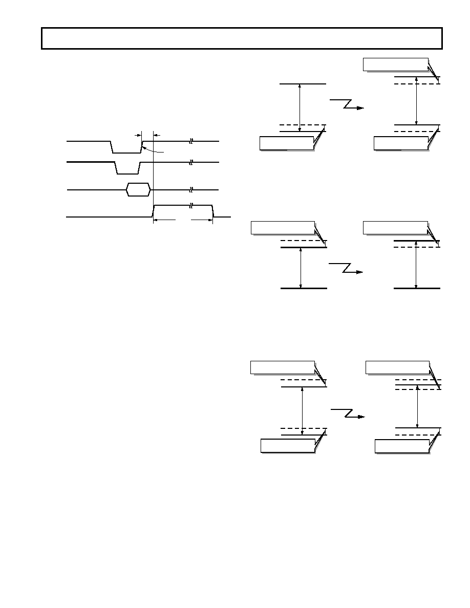
Figures 30 through 32 illustrate why a specific type of system
calibration might be used. Figure 30 shows a system offset cali-
bration (assuming a positive offset) where the analog input
range has been shifted upwards by the system offset after the
system offset calibration is completed. A negative offset may
also be removed by a system offset calibration.
MAX SYSTEM OFFSET
IS ±5% OF VREF
ANALOG
INPUT
RANGE
SYSTEM OFFSET
CALIBRATION
SYS OFFSET
AGND
VREF + SYS OFFSET
VREF – 1LSB
MAX SYSTEM FULL SCALE
IS ±2.5% FROM VREF
ANALOG
INPUT
RANGE
MAX SYSTEM OFFSET
IS ±5% OF VREF
VREF – 1LSB
SYS OFFSET
AGND
Figure 30. System Offset Calibration
Figure 31 shows a system gain calibration (assuming a system
full scale greater than the reference voltage) where the analog
input range has been increased after the system gain calibration
is completed. A system full-scale voltage less than the reference
voltage may also be accounted for a by a system gain calibration.
ANALOG
INPUT
RANGE
SYSTEM OFFSET
CALIBRATION
AGND
SYS FULL S.
VREF – 1LSB
MAX SYSTEM FULL SCALE
IS ±2.5% FROM VREF
ANALOG
INPUT
RANGE
VREF – 1LSB
SYS FULL S.
AGND
MAX SYSTEM FULL SCALE
IS ±2.5% FROM VREF
Figure 31. System Gain Calibration
Finally in Figure 32 both the system offset error and gain error
are removed by the system offset followed by a system gain cali-
bration. First the analog input range is shifted upwards by the
positive system offset and then the analog input range is
adjusted at the top end to account for the system full scale.
MAX SYSTEM FULL SCALE
IS ±2.5% FROM VREF
MAX SYSTEM OFFSET
IS ±5% OF VREF
ANALOG
INPUT
RANGE
SYSTEM OFFSET
CALIBRATION
FOLLOWED BY
SYSTEM GAIN
CALIBRATION SYS OFFSET
AGND
VREF + SYS OFFSET
VREF – 1LSB
ANALOG
INPUT
RANGE
MAX SYSTEM OFFSET
IS ±5% OF VREF
VREF – 1LSB
SYS OFFSET
AGND
SYS F.S.
MAX SYSTEM FULL SCALE
IS ±2.5% FROM VREF
Figure 32. System (Gain + Offset) Calibration
相关PDF资料 |
PDF描述 |
|---|---|
| MS3106A16S-6P | CONN PLUG 3POS STRAIGHT W/PINS |
| MS3102R20-19P | CONN RCPT 3POS BOX MNT W/PINS |
| AD7895ARZ-3 | IC ADC 12BIT SRL 5V 8-SOIC |
| VI-B50-IV-F4 | CONVERTER MOD DC/DC 5V 150W |
| AD7706BNZ | IC ADC 16BIT 3CHAN 16DIP |
相关代理商/技术参数 |
参数描述 |
|---|---|
| AD7854LARZ-REEL | 功能描述:IC ADC 12BIT PARALLEL LP 28SOIC RoHS:是 类别:集成电路 (IC) >> 数据采集 - 模数转换器 系列:- 标准包装:1,000 系列:- 位数:16 采样率(每秒):45k 数据接口:串行 转换器数目:2 功率耗散(最大):315mW 电压电源:模拟和数字 工作温度:0°C ~ 70°C 安装类型:表面贴装 封装/外壳:28-SOIC(0.295",7.50mm 宽) 供应商设备封装:28-SOIC W 包装:带卷 (TR) 输入数目和类型:2 个单端,单极 |
| AD7854LBR | 制造商:未知厂家 制造商全称:未知厂家 功能描述:Analog-to-Digital Converter, 12-Bit |
| AD7854SQ | 制造商:Rochester Electronics LLC 功能描述:12-BIT SINGLE CH.PARALLEL ADC I.C. - Bulk |
| AD7856 | 制造商:AD 制造商全称:Analog Devices 功能描述:5 V Single Supply, 8-Channel 14-Bit 285 kSPS Sampling ADC |
| AD7856AN | 制造商:Analog Devices 功能描述:ADC Single SAR 285ksps 14-bit Serial 24-Pin PDIP 制造商:Analog Devices 功能描述:IC 14BIT ADC 7856 DIP24 |
发布紧急采购,3分钟左右您将得到回复。