- 您现在的位置:买卖IC网 > PDF目录10180 > AD7858AR (Analog Devices Inc)IC ADC 12BIT 8CH SRL 24-SOIC PDF资料下载
参数资料
| 型号: | AD7858AR |
| 厂商: | Analog Devices Inc |
| 文件页数: | 14/32页 |
| 文件大小: | 0K |
| 描述: | IC ADC 12BIT 8CH SRL 24-SOIC |
| 标准包装: | 31 |
| 位数: | 12 |
| 采样率(每秒): | 200k |
| 数据接口: | 8051,QSPI?,串行,SPI? µP |
| 转换器数目: | 2 |
| 功率耗散(最大): | 33mW |
| 电压电源: | 模拟和数字 |
| 工作温度: | -40°C ~ 85°C |
| 安装类型: | 表面贴装 |
| 封装/外壳: | 24-SOIC(0.295",7.50mm 宽) |
| 供应商设备封装: | 24-SOIC W |
| 包装: | 管件 |
| 输入数目和类型: | 8 个单端,单极;4 个伪差分,单极 |
第1页第2页第3页第4页第5页第6页第7页第8页第9页第10页第11页第12页第13页当前第14页第15页第16页第17页第18页第19页第20页第21页第22页第23页第24页第25页第26页第27页第28页第29页第30页第31页第32页
AD7858/AD7858L
REV. B
–21–
Automatic Calibration on Power-On
The
CAL pin has a 0.15
A pull-up current source connected
to it internally to allow for an automatic full self-calibration on
power-on. A full self-calibration will be initiated on power-on if
a capacitor is connected from the
CAL pin to DGND. The
internal current source connected to the
CAL pin charges up
the external capacitor and the time required to charge the exter-
nal capacitor will depend on the size of the capacitor itself. This
time should be large enough to ensure that the internal refer-
ence is settled before the calibration is performed. A 33 nF
capacitor is sufficient to ensure that the internal reference has
settled (see Power-Up Times) before a calibration is initiated
taking into account trigger level and current source variations
on the
CAL pin. However, if an external reference is being
used, this reference must have stabilized before the automatic
calibration is initiated (a larger capacitor on the
CAL pin
should be used if the external reference has not settled when the
autocalibration is initiated). Once the capacitor on the
CAL pin
has charged, the calibration will be performed which will take
32 ms (4 MHz CLKIN). Therefore the autocalibration should
be complete before operating the part. After calibration, the
part is accurate to the 12-bit level and the specifications quoted
on the data sheet apply. There will be no need to perform
another calibration unless the operating conditions change or
unless a system calibration is required.
Self-Calibration Description
There are four different calibration options within the self-
calibration mode. First, there is a full self-calibration where the
DAC, internal gain, and internal offset errors are calibrated out.
Then, there is the (Gain + Offset) self-calibration which cali-
brates out the internal gain error and then the internal offset
errors. The internal DAC is not calibrated here. Finally, there
are the self-offset and self-gain calibrations which calibrate out
the internal offset errors and the internal gain errors respectively.
The internal capacitor DAC is calibrated by trimming each of
the capacitors in the DAC. It is the ratio of these capacitors to
each other that is critical, and so the calibration algorithm en-
sures that this ratio is at a specific value by the end of the cali-
bration routine. For the offset and gain there are two separate
capacitors, one of which is trimmed when an offset or gain
calibration is performed. Again, it is the ratio of these capacitors
to the capacitors in the DAC that is critical and the calibration
algorithm ensures that this ratio is at a specified value for both
the offset and gain calibrations.
The zero-scale error is adjusted for an offset calibration, and
the positive full-scale error is adjusted for a gain calibration.
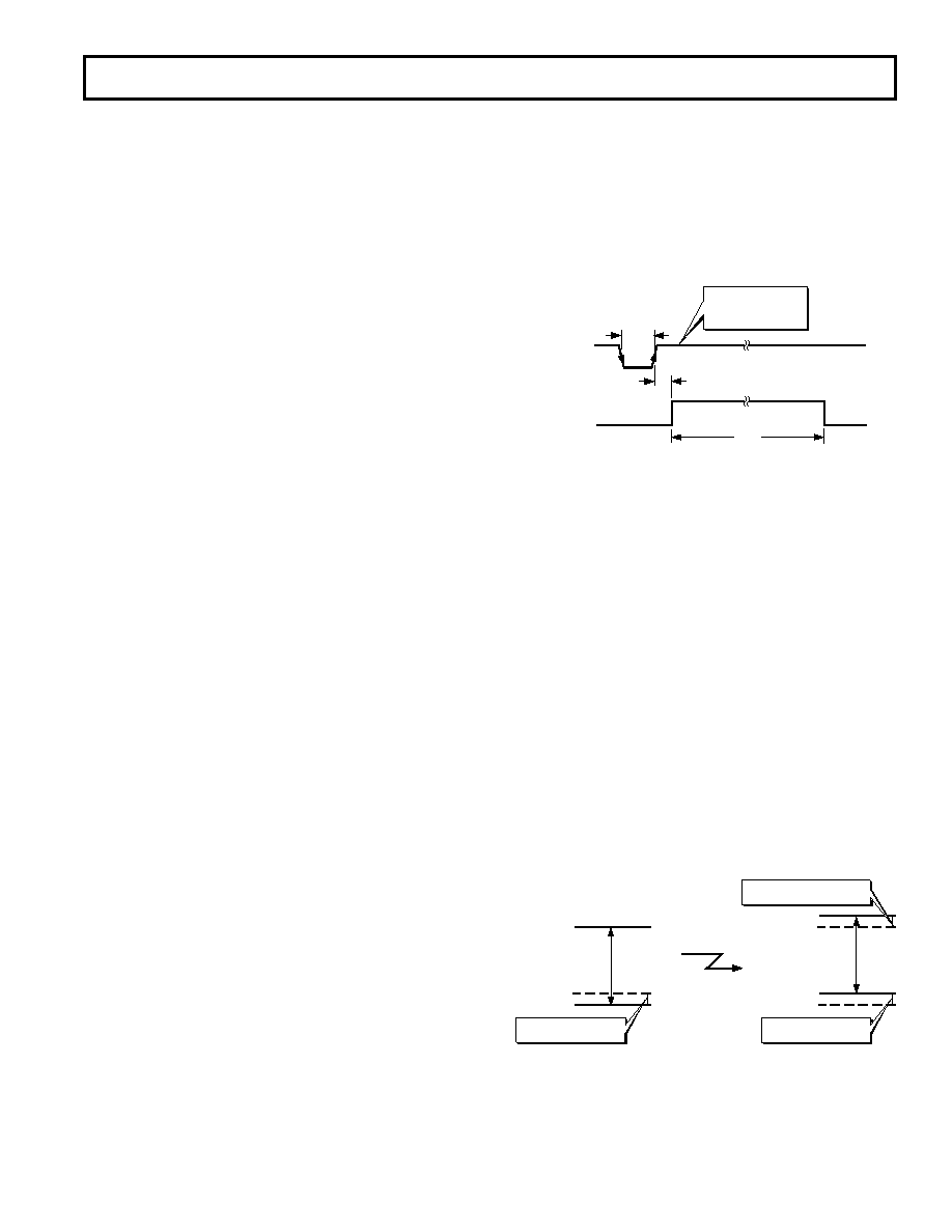
Self-Calibration Timing
The diagram of Figure 25 shows the timing for a full self-
calibration. Here the BUSY line stays high for the full length of
the self-calibration. A self-calibration is initiated by bringing the
CAL pin low (which initiates an internal reset) and then high
again or by writing to the control register and setting the STCAL
bit to 1 (note that if the part is in a power-down mode the
CAL pulse-
width must take account of the power-up time ). The BUSY line is
triggered high from the rising edge of
CAL (or the end of the
write to the control register if calibration is initiated in soft-
ware), and BUSY will go low when the full self-calibration is
complete after a time tCAL as shown in Figure 25.
For the self- (gain + offset), self-offset, and self-gain calibrations
the BUSY line will be triggered high by the rising edge of the
CAL signal (or the end of the write to the control register if
calibration is initiated in software) and will stay high for the
full duration of the self-calibration. The length of time that
the BUSY is high will depend on the type of self-calibration
that is initiated. Typical figures are given in Table VIII. The
timing diagrams for the other self-calibration options will be
similar to that outlined in Figure 25.
t1 = 100ns MIN,
t15 = 2.5 tCLKIN MAX,
tCAL = 125013 tCLKIN
t1
t15
tCAL
BUSY (O/P)
CAL (I/P)
Figure 25. Timing Diagram for Full Self-Calibration
System Calibration Description
System calibration allows the user to take out system errors
external to the AD7858/AD7858L as well as calibrate the errors
of the AD7858/AD7858L itself. The maximum calibration
range for the system offset errors is
±5% of VREF and for the
system gain errors is
±2.5% of V
REF. This means that the maxi-
mum allowable system offset voltage applied between the
AIN(+) and AIN(–) pins for the calibration to adjust out this
error is
±0.05 × V
REF (i.e., the AIN(+) can be 0.05
× V
REF above
AIN(–) or 0.05
× V
REF below AIN(–)). For the System gain error
the maximum allowable system full-scale voltage that can be
applied between AIN(+) and AIN(–) for the calibration to
adjust out this error is VREF
± 0.025
× V
REF ( i.e., the AIN(+)
above AIN(–)). If the system offset or system gain errors are
outside the ranges mentioned the system calibration algorithm
will reduce the errors as much as the trim range allows.
Figures 26 through 28 illustrate why a specific type of system
calibration might be used. Figure 26 shows a system offset
calibration (assuming a positive offset) where the analog input
range has been shifted upwards by the system offset after the
system offset calibration is completed. A negative offset may
also be accounted for by a system offset calibration.
MAX SYSTEM OFFSET
IS
5% OF VREF
VREF –1LSB
SYS OFFSET
AGND
ANALOG
INPUT
RANGE
MAX SYSTEM FULL SCALE
IS
2.5% FROM VREF
SYSTEM OFFSET
CALIBRATION
MAX SYSTEM OFFSET
IS
5% OF VREF
SYS OFFSET
AGND
VREF + SYS OFFSET
VREF – 1LSB
ANALOG
INPUT
RANGE
Figure 26. System Offset Calibration
相关PDF资料 |
PDF描述 |
|---|---|
| ADM211EARUZ-REEL | IC TXRX RS-232 5V 0.1UF 28TSSOP |
| ADM213EARUZ-REEL | IC TXRX RS-232 5V 0.1UF 28TSSOP |
| MS27474T8B35S | CONN RCPT 6POS JAM NUT W/SCKT |
| MS3108E14S-5S | CONN PLUG 5POS RT ANG W/SCKT |
| MS27472E12A98PA | CONN RCPT 10POS WALL MT W/PINS |
相关代理商/技术参数 |
参数描述 |
|---|---|
| AD7858AR-REEL | 制造商:Analog Devices 功能描述:ADC Single SAR 200ksps 12-bit Serial 24-Pin SOIC W T/R 制造商:Analog Devices 功能描述:ADC SGL SAR 200KSPS 12-BIT SERL 24SOIC W - Tape and Reel 制造商:Rochester Electronics LLC 功能描述:SELF CAL.SERIAL 8CH. 12-BIT ADC I.C. - Tape and Reel |
| AD7858ARZ | 功能描述:IC ADC 12BIT 8CH SRL 24-SOIC RoHS:是 类别:集成电路 (IC) >> 数据采集 - 模数转换器 系列:- 其它有关文件:TSA1204 View All Specifications 标准包装:1 系列:- 位数:12 采样率(每秒):20M 数据接口:并联 转换器数目:2 功率耗散(最大):155mW 电压电源:模拟和数字 工作温度:-40°C ~ 85°C 安装类型:表面贴装 封装/外壳:48-TQFP 供应商设备封装:48-TQFP(7x7) 包装:Digi-Reel® 输入数目和类型:4 个单端,单极;2 个差分,单极 产品目录页面:1156 (CN2011-ZH PDF) 其它名称:497-5435-6 |
| AD7858ARZ-REEL | 功能描述:IC ADC 12BIT 8CHAN SRL 24SOIC RoHS:是 类别:集成电路 (IC) >> 数据采集 - 模数转换器 系列:- 标准包装:1,000 系列:- 位数:12 采样率(每秒):300k 数据接口:并联 转换器数目:1 功率耗散(最大):75mW 电压电源:单电源 工作温度:0°C ~ 70°C 安装类型:表面贴装 封装/外壳:24-SOIC(0.295",7.50mm 宽) 供应商设备封装:24-SOIC 包装:带卷 (TR) 输入数目和类型:1 个单端,单极;1 个单端,双极 |
| AD7858BN | 制造商:AD 制造商全称:Analog Devices 功能描述:3 V to 5 V Single Supply, 200 kSPS 8-Channel, 12-Bit Sampling ADC |
| AD7858BNZ | 功能描述:IC ADC 12BIT 8CHAN SRL 24DIP RoHS:是 类别:集成电路 (IC) >> 数据采集 - 模数转换器 系列:- 产品培训模块:Lead (SnPb) Finish for COTS Obsolescence Mitigation Program 标准包装:2,500 系列:- 位数:12 采样率(每秒):3M 数据接口:- 转换器数目:- 功率耗散(最大):- 电压电源:- 工作温度:- 安装类型:表面贴装 封装/外壳:SOT-23-6 供应商设备封装:SOT-23-6 包装:带卷 (TR) 输入数目和类型:- |
发布紧急采购,3分钟左右您将得到回复。