参数资料
| 型号: | AD7859BSZ |
| 厂商: | Analog Devices Inc |
| 文件页数: | 22/28页 |
| 文件大小: | 0K |
| 描述: | IC ADC 12BIT 8CHAN LP 44-MQFP |
| 标准包装: | 1 |
| 位数: | 12 |
| 采样率(每秒): | 200k |
| 数据接口: | 并联 |
| 转换器数目: | 2 |
| 功率耗散(最大): | 30mW |
| 电压电源: | 模拟和数字 |
| 工作温度: | -40°C ~ 85°C |
| 安装类型: | 表面贴装 |
| 封装/外壳: | 44-QFP |
| 供应商设备封装: | 44-MQFP(10x10) |
| 包装: | 托盘 |
| 输入数目和类型: | 8 个单端,单极;8 个单端,双极;4 个伪差分,单极;4 个伪差分,双极 |
第1页第2页第3页第4页第5页第6页第7页第8页第9页第10页第11页第12页第13页第14页第15页第16页第17页第18页第19页第20页第21页当前第22页第23页第24页第25页第26页第27页第28页
REV. A
–3–
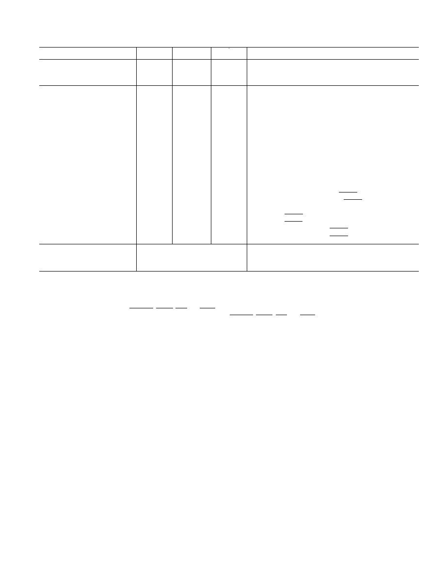
Parameter
A Version1
B Version1
Units
Test Conditions/Comments
CONVERSION RATE
tCLKIN × 18
Conversion Time
4.5 (10)
4.5
s max
(L Versions Only, 0
°C to +70°C, 1.8 MHz CLKIN)
Track/Hold Acquisition Time
0.5 (1)
0.5
s min
(L Versions Only, –40
°C to +85°C, 1.8 MHz CLKIN)
POWER REQUIREMENTS
AVDD, DVDD
+3.0/+5.5
V min/max
IDD
Normal Mode
5
5.5 (1.95)
5.5
mA max
AVDD = DVDD = 4.5 V to 5.5 V. Typically 4.5 mA
5.5 (1.95)
5.5
mA max
AVDD = DVDD = 3.0 V to 3.6 V. Typically 4.0 mA
Sleep Mode
6
With External Clock On
10
A typ
Full Power-Down. Power Management Bits in Control
Register Set as PMGT1 = 1, PMGT0 = 0.
400
A typ
Partial Power-Down. Power Management Bits in
Control Register Set as PMGT1 = 1, PMGT0 = 1.
With External Clock Off
5
A max
Typically 1
A. Full Power-Down. Power Management
Bits in Control Register Set as PMGT1 = 1, PMGT0 = 0.
200
A typ
Partial Power-Down. Power Management Bits in
Control Register Set as PMGT1 = 1, PMGT0 = 1.
Normal Mode Power Dissipation
30 (10)
mW max
VDD = 5.5 V: Typically 25 mW (8); SLEEP = VDD
20 (6.5)
mW max
VDD = 3.6 V: Typically 15 mW (5.4); SLEEP = VDD
Sleep Mode Power Dissipation
With External Clock On
55
W typ
VDD = 5.5 V; SLEEP = 0 V
36
W typ
VDD = 3.6 V; SLEEP = 0 V
With External Clock Off
27.5
W max
VDD = 5.5 V: Typically 5.5 W; SLEEP = 0 V
18
W max
VDD = 3.6 V: Typically 3.6
W; SLEEP = 0 V
SYSTEM CALIBRATION
Offset Calibration Span
7
+0.05
× V
REF/–0.05 × VREF
V max/min
Allowable Offset Voltage Span for Calibration
Gain Calibration Span
7
+1.025
× V
REF/–0.975
× V
REF V max/min
Allowable Full-Scale Voltage Span for Calibration
NOTES
1Temperature range as follows: A, B Versions, –40
°C to +85°C.
2Specifications apply after calibration.
3SNR calculation includes distortion and noise components.
4Not production tested, guaranteed by characterization at initial product release.
5All digital inputs @ DGND except for CONVST, SLEEP, CAL, and SYNC @ DV
DD. No load on the digital outputs. Analog inputs @ AGND.
6CLKIN @ DGND when external clock off. All digital inputs @ DGND except for CONVST, SLEEP, CAL, and SYNC @ DV
DD. No load on the digital outputs.
Analog inputs @ AGND.
7The offset and gain calibration spans are defined as the range of offset and gain errors that the AD7859/AD7859L can calibrate. Note also that these are voltage spans
and are not absolute voltages (i.e., the allowable system offset voltage presented at AIN(+) for the system offset error to be adjusted out will be AIN(–)
± 0.05 × V
REF,
and the allowable system full-scale voltage applied between AIN(+) and AIN(–) for the system full-scale voltage error to be adjusted out will be VREF
± 0.025 × V
REF).
This is explained in more detail in the calibration section of the data sheet.
Specifications subject to change without notice.
AD7859/AD7859L
相关PDF资料 |
PDF描述 |
|---|---|
| AD7861AP | IC ADC 11BIT 4CH 44-PLCC |
| AD7862BRZ-10 | IC ADC 12BIT DUAL 250KSPS 28SOIC |
| AD7863ARZ-10REEL | IC ADC 14BIT DUAL 2CH 28-SOIC |
| AD7864BSZ-1REEL | IC ADC 12BIT DUAL 4CHAN 44-MQFP |
| AD7865YSZ-3 | IC ADC 14BIT 4CHAN 5V 44-MQFP |
相关代理商/技术参数 |
参数描述 |
|---|---|
| AD7859L | 制造商:AD 制造商全称:Analog Devices 功能描述:3 V to 5 V Single Supply, 200 kSPS 8-Channel, 12-Bit Sampling ADCs |
| AD7859LAS | 制造商:Analog Devices 功能描述:ADC Single SAR 100ksps 12-bit Parallel 44-Pin MQFP 制造商:Rochester Electronics LLC 功能描述:12-BIT 8 CH.PARALLEL 100 KSPS I.C. - Bulk 制造商:Analog Devices 功能描述:IC 12-BIT ADC |
| AD7859LAS3 | 制造商:AD 制造商全称:Analog Devices 功能描述:3 V to 5 V Single Supply, 200 kSPS8-Channel, 12-Bit Sampling ADCs |
| AD7859LAS-REEL | 制造商:Analog Devices 功能描述:ADC Single SAR 100ksps 12-bit Parallel 44-Pin MQFP T/R |
发布紧急采购,3分钟左右您将得到回复。