- 您现在的位置:买卖IC网 > PDF目录10661 > AD7865ASZ-1 (Analog Devices Inc)IC ADC 14BIT DUAL 4CH 44-MQFP PDF资料下载
参数资料
| 型号: | AD7865ASZ-1 |
| 厂商: | Analog Devices Inc |
| 文件页数: | 5/19页 |
| 文件大小: | 0K |
| 描述: | IC ADC 14BIT DUAL 4CH 44-MQFP |
| 标准包装: | 1 |
| 位数: | 14 |
| 采样率(每秒): | 350k |
| 数据接口: | 并联 |
| 转换器数目: | 1 |
| 功率耗散(最大): | 160mW |
| 电压电源: | 模拟和数字 |
| 工作温度: | -40°C ~ 85°C |
| 安装类型: | 表面贴装 |
| 封装/外壳: | 44-QFP |
| 供应商设备封装: | 44-MQFP(10x10) |
| 包装: | 托盘 |
| 输入数目和类型: | 4 个差分,双极 |
| 产品目录页面: | 779 (CN2011-ZH PDF) |
REV. B
AD7865
–13–
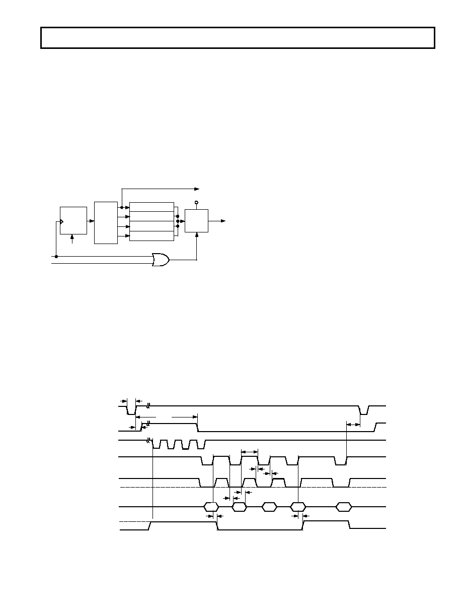
Accessing the Output Data Registers
There are four Output Data Registers, one for each of the four
possible conversion results from a conversion sequence. The
result of the first conversion in a conversion sequence is placed
in Register 1 and the second result is placed in Register 2 and so
on. For example if the conversion sequence VIN1, VIN3 and VIN4
is selected (see Selecting a Conversion Sequence) the results of
the conversion on VIN1, VIN3 and VIN4 are placed in Registers 1
to 3 respectively. The Output Data register pointer is reset to
point to Register 1 at the end of the first conversion in the
sequence, just prior to
EOC going low. At this point the logic
output FRSTDATA will go logic high to indicate that the out-
put data register pointer is addressing Register 1. When
CS and
RD are both logic low the contents of the addressed register are
enabled onto the data bus (DB0–DB13).
DB0 TO
DB13
O/P
DRIVERS
OE #1
NOT VALID
(VIN3)
(VIN1)
(VIN4)
OE #2
OE #3
OE #4
2-BIT
COUNTER
VDRIVE
OE
RD
CS
RESET
OUTPUT
DATA REGISTERS
*THE POINTER WILL NOT BE INCREMENTED BY A RISING EDGE ON
RD UNTIL
THE CONVERSION RESULT IS IN THE OUTPUT DATA REGISTER. THE POINTER
IS RESET WHEN THE LAST CONVERSION RESULT IS READ
FRSTDATA
POINTER*
AD7865
DECODE
Figure 8. Output Data Registers
When reading the output data registers after a conversion
sequence, i.e., when BUSY goes low, the register pointer is
incremented on the rising edge of the
RD signal as shown in
Figure 8. However, when reading the conversion results between
conversions in a conversion sequence the pointer will not be
incremented until a valid conversion result is in the register to
be addressed. In this case the pointer is incremented when the
conversion has ended and the result has been transferred to the
output data register. This happens when
EOC goes low, there-
fore
EOC may be used to enable the register contents onto the
data bus as described in Reading Between Conversions in the
Conversion Sequence. The pointer is reset to point to Register 1
on the rising edge of the
RD signal when the last conversion
result in the sequence is being read. In the example shown in
Figure 8, this means that the pointer is set to Register 1 when
the contents of Register 3 are read.
Reading after the Conversion Sequence
Figure 9 shows the same conversion sequence as Figure 7. In
this case, however, the results of the four conversions (on VIN1
to VIN4) are read after all conversions have finished, i.e., when
BUSY goes logic low. The FRSTDATA signal goes logic high
at the end of the first conversion just prior to
EOC going logic
low. As mentioned previously FRSTDATA has an indetermi-
nate state after initial power up, therefore FRSTDATA may
already be logic high. Unlike the case when reading during a
conversion the output data register pointer is incremented on
the rising edge of
RD because the next conversion result is avail-
able in this case. This means FRSTDATA will go logic low after
the first rising edge on
RD.
Successive read operations will access the remaining conversion
results in ascending channel order. Each read operation incre-
ments the output data register pointer. The read operation that
accesses the last conversion result causes the output data regis-
ter pointer to be reset so that the next read operation will access
the first conversion result again. This is shown in Figure 8 with
the fifth read after BUSY goes low accessing the result of the
conversion on VIN1. Thus the output data registers acts as a
circular buffer in which the conversion results may be continu-
ally accessed. The FRSTDATA signal will go high when the
first conversion result is available.
Data is enabled onto the data bus DB0 to DB13 using
CS and
RD. Both CS and RD have the same functionality as described
in the previous section. There are no restrictions or performance
implications associated with the position of the read operations
after BUSY goes low, however there is a minimum time between
read operations that must be adhered to. Notice also that a “Quiet
Time” is needed before the start of the next conversion sequence.
t10
t8
t4
t3
t6
t1
QUIET
TIME
DATA
CONVST
BUSY
EOC
FRSTDATA
RD
CS
VIN2
VIN3
VIN1
tBUSY
t2
t10
t7
VIN1
VIN4
Figure 9. Timing Diagram, Reading after the Conversion Sequences
相关PDF资料 |
PDF描述 |
|---|---|
| MAX972CPA+ | IC COMPARATOR OD 8-DIP |
| VI-J13-MW-F3 | CONVERTER MOD DC/DC 24V 100W |
| LTC2245IUH#PBF | IC ADC 14-BIT 10MSPS 3V 32-QFN |
| MAX917ESA+ | IC COMPARATOR BTR 8-SOIC |
| AD9225ARSZ | IC ADC 12BIT 25MSPS 28-SSOP |
相关代理商/技术参数 |
参数描述 |
|---|---|
| AD7865ASZ-1REEL | 功能描述:IC ADC 14BIT 4CHAN 5V 44-MQFP RoHS:是 类别:集成电路 (IC) >> 数据采集 - 模数转换器 系列:- 标准包装:1,000 系列:- 位数:12 采样率(每秒):300k 数据接口:并联 转换器数目:1 功率耗散(最大):75mW 电压电源:单电源 工作温度:0°C ~ 70°C 安装类型:表面贴装 封装/外壳:24-SOIC(0.295",7.50mm 宽) 供应商设备封装:24-SOIC 包装:带卷 (TR) 输入数目和类型:1 个单端,单极;1 个单端,双极 |
| AD7865ASZ-2 | 功能描述:IC ADC 14BIT 4CHAN 5V 44MQFP RoHS:是 类别:集成电路 (IC) >> 数据采集 - 模数转换器 系列:- 标准包装:1 系列:- 位数:14 采样率(每秒):83k 数据接口:串行,并联 转换器数目:1 功率耗散(最大):95mW 电压电源:双 ± 工作温度:0°C ~ 70°C 安装类型:通孔 封装/外壳:28-DIP(0.600",15.24mm) 供应商设备封装:28-PDIP 包装:管件 输入数目和类型:1 个单端,双极 |
| AD7865ASZ-2REEL | 功能描述:IC ADC 14BIT 4CHAN 5V 44-MQFP RoHS:是 类别:集成电路 (IC) >> 数据采集 - 模数转换器 系列:- 标准包装:1,000 系列:- 位数:12 采样率(每秒):300k 数据接口:并联 转换器数目:1 功率耗散(最大):75mW 电压电源:单电源 工作温度:0°C ~ 70°C 安装类型:表面贴装 封装/外壳:24-SOIC(0.295",7.50mm 宽) 供应商设备封装:24-SOIC 包装:带卷 (TR) 输入数目和类型:1 个单端,单极;1 个单端,双极 |
| AD7865ASZ-3 | 功能描述:IC ADC 14BIT 4CHAN 5V 44MQFP RoHS:是 类别:集成电路 (IC) >> 数据采集 - 模数转换器 系列:- 其它有关文件:TSA1204 View All Specifications 标准包装:1 系列:- 位数:12 采样率(每秒):20M 数据接口:并联 转换器数目:2 功率耗散(最大):155mW 电压电源:模拟和数字 工作温度:-40°C ~ 85°C 安装类型:表面贴装 封装/外壳:48-TQFP 供应商设备封装:48-TQFP(7x7) 包装:Digi-Reel® 输入数目和类型:4 个单端,单极;2 个差分,单极 产品目录页面:1156 (CN2011-ZH PDF) 其它名称:497-5435-6 |
| AD7865ASZ-3REEL | 功能描述:IC ADC 14BIT 4CHAN 5V 44-MQFP RoHS:是 类别:集成电路 (IC) >> 数据采集 - 模数转换器 系列:- 标准包装:1,000 系列:- 位数:12 采样率(每秒):300k 数据接口:并联 转换器数目:1 功率耗散(最大):75mW 电压电源:单电源 工作温度:0°C ~ 70°C 安装类型:表面贴装 封装/外壳:24-SOIC(0.295",7.50mm 宽) 供应商设备封装:24-SOIC 包装:带卷 (TR) 输入数目和类型:1 个单端,单极;1 个单端,双极 |
发布紧急采购,3分钟左右您将得到回复。