- 您现在的位置:买卖IC网 > PDF目录10531 > AD7865ASZ-3 (Analog Devices Inc)IC ADC 14BIT 4CHAN 5V 44MQFP PDF资料下载
参数资料
| 型号: | AD7865ASZ-3 |
| 厂商: | Analog Devices Inc |
| 文件页数: | 4/19页 |
| 文件大小: | 0K |
| 描述: | IC ADC 14BIT 4CHAN 5V 44MQFP |
| 标准包装: | 1 |
| 位数: | 14 |
| 采样率(每秒): | 350k |
| 数据接口: | 并联 |
| 转换器数目: | 1 |
| 功率耗散(最大): | 160mW |
| 电压电源: | 模拟和数字 |
| 工作温度: | -40°C ~ 85°C |
| 安装类型: | 表面贴装 |
| 封装/外壳: | 44-QFP |
| 供应商设备封装: | 44-MQFP(10x10) |
| 包装: | 托盘 |
| 输入数目和类型: | 4 个差分,双极 |
REV. B
AD7865
–12–
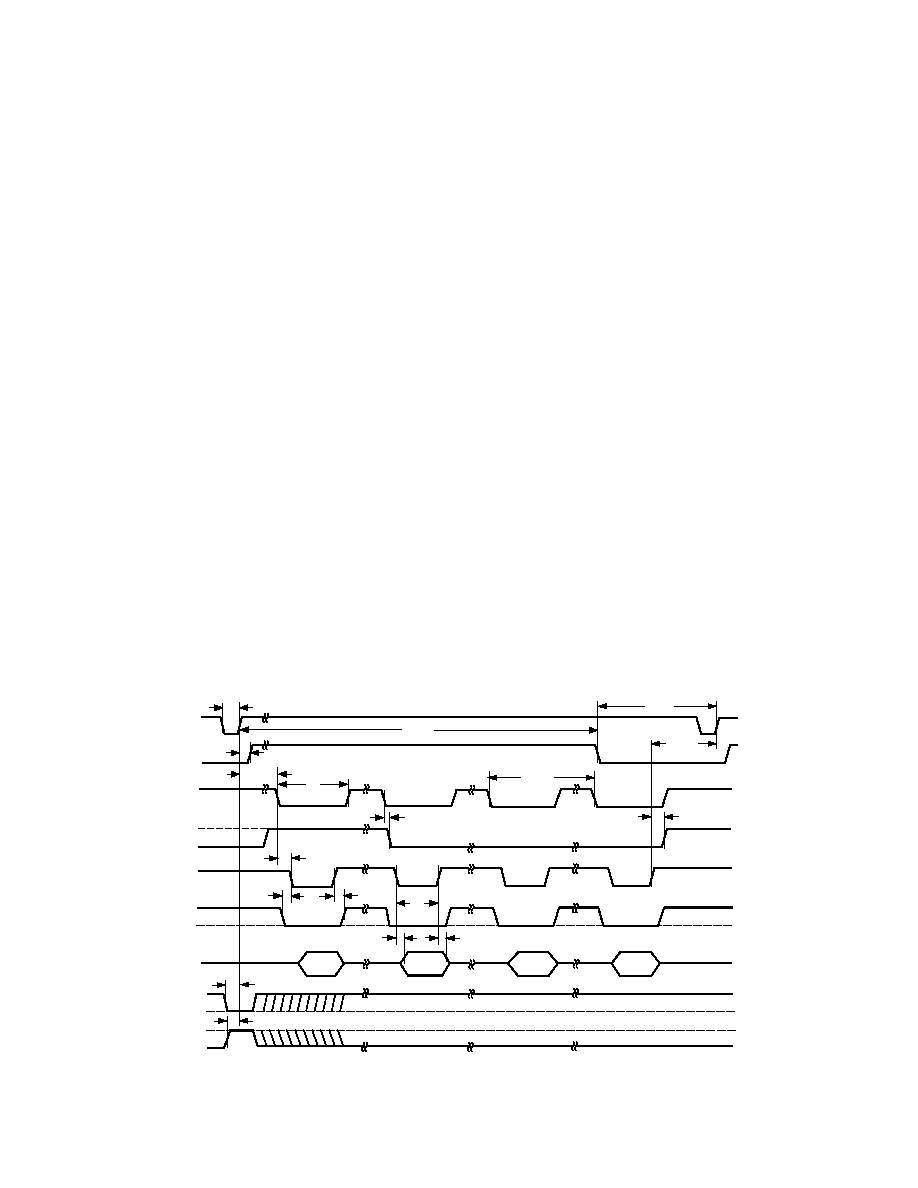
TIMING AND CONTROL
Reading Between Each Conversion in the Conversion Sequence
Figure 7 shows the timing and control sequence required to
obtain the optimum throughput rate from the AD7865. To
obtain the optimum throughput from the AD7865 the user must
read the result of each conversion as it becomes available. The
timing diagram in Figure 7 shows a read operation each time the
EOC signal goes logic low. The timing in Figure 7 shows a
conversion on all four analog channels (SL1 to SL4 = 1, see
Selecting a Conversion Sequence), hence there are four
EOC
pulses and four read operations to access the result of each of
the four conversions.
A conversion is initiated on the rising edge of
CONVST. This
places all four track/holds into hold simultaneously. New data
from this conversion sequence is available for the first channel
selected (AIN1) 2.4
s later. The conversion on each subsequent
channel is completed at 2.4
s intervals. The end of each con-
version is indicated by the falling edge of the
EOC signal. The
BUSY output signal indicates the end of conversion for all
selected channels (four in this case).
Data is read from the part via a 14-bit parallel data bus with
standard
CS and RD signals. The CS and RD inputs are inter-
nally gated to enable the conversion result onto the data bus.
The data lines DB0 to DB13 leave their high impedance state
when both
CS and RD are logic low. Therefore, CS may be
permanently tied logic low and the
RD signal used to access the
conversion result. Since each conversion result is latched into its
output data register at the same time
EOC goes logic low a
further option would be to tie the
EOC and RD pins together
with
CS tied logic low and use the rising edge of EOC to latch
the conversion result. Although the AD7865 has some special
features that permit reading during a conversion (e.g., a sepa-
rate supply for the output data drivers, VDRIVE), for optimum
performance it is recommended that the read operation be
completed when
EOC is logic low, i.e., before the start of the
next conversion. Although Figure 7 shows the read operation
taking place during the
EOC pulse, a read operation can take
place at any time. Figure 7 shows a timing specification called
“Quiet Time.” This is the amount of time that should be left
after a read operation and before the next conversion is initi-
ated. The quiet time heavily depends on data bus capacitance
but a figure of 50 ns to 150 ns is typical.
The signal labeled FRSTDATA (First Data Word) indicates to
the user that the pointer associated with the output data regis-
ters is pointing to the first conversion result by going logic high.
The pointer is reset to point to the first data location (i.e., first
conversion result,) at the end of the first conversion just prior to
EOC going low. The pointer is incremented to point to the next
register (next conversion result) by a rising edge of
RD only if
that conversion result is available. If a read takes place before
the next conversion is complete (as shown in Figure 7) then the
pointer is incremented at the end of that conversion when the
EOC pulse goes low. Hence, FRSTDATA in Figure 7 is seen to
go low just after to the second
EOC pulse. Repeated read
operations during a conversion will continue to access the data
at the current pointer location until the pointer is incremented
at the end of that conversion. Note: FRSTDATA has an indeter-
minate logic state after initial power-up. This means that for the
first conversion sequence after power-up, the FRSTDATA
logic output may already be logic high before the end of the first
conversion. This condition is indicated by the dashed line in
Figure 7. Also the FRSTDATA logic output may already be
high as a result of the previous read sequence as is the case after
the fourth read in Figure 7. The fourth read (rising edge of
RD)
resets the pointer to the first data location. There, however,
FRSTDATA is already high when the next conversion sequence
is initiated.
QUIET
TIME
tCONV
tBUSY
t1
t12
t3
t4
t5
t6
t7
VIN1
VIN2
VIN3
VIN4
100ns
DATA
CONVST
BUSY
EOC
FRSTDATA
RD
CS
H/S SEL
SL1–SL4
t2
tACQ
t11
t10
tCONV
t9
Figure 7. Timing Diagram for Reading During Conversion
相关PDF资料 |
PDF描述 |
|---|---|
| MS3100A18-6P | CONN RCPT 1POS WALL MNT W/PINS |
| VI-J42-MW-F3 | CONVERTER MOD DC/DC 15V 100W |
| LTC1856CG#PBF | IC ADC 16BIT 100KSPS 28-SSOP |
| MS3102A24-16P | CONN RCPT 7POS BOX MNT W/PINS |
| VI-J42-MW-F1 | CONVERTER MOD DC/DC 15V 100W |
相关代理商/技术参数 |
参数描述 |
|---|---|
| AD7865ASZ-3REEL | 功能描述:IC ADC 14BIT 4CHAN 5V 44-MQFP RoHS:是 类别:集成电路 (IC) >> 数据采集 - 模数转换器 系列:- 标准包装:1,000 系列:- 位数:12 采样率(每秒):300k 数据接口:并联 转换器数目:1 功率耗散(最大):75mW 电压电源:单电源 工作温度:0°C ~ 70°C 安装类型:表面贴装 封装/外壳:24-SOIC(0.295",7.50mm 宽) 供应商设备封装:24-SOIC 包装:带卷 (TR) 输入数目和类型:1 个单端,单极;1 个单端,双极 |
| AD7865ASZ-3REEL-SCHNEIDER | 制造商:Analog Devices 功能描述: |
| AD7865BS-1 | 制造商:Rochester Electronics LLC 功能描述:4 CH. SIMULTANEOUS BIPOLAR,14-B ADC I.C. - Bulk 制造商:Analog Devices 功能描述:IC 14-BIT ADC |
| AD7865BS-1Z | 制造商:Analog Devices 功能描述:ADC 14BIT 4CH 350KSPS 44LQ 制造商:Analog Devices 功能描述:ADC, 14BIT, 4CH, 350KSPS, 44LQFP; Resolution (Bits):14bit; Sampling Rate:350kSPS; Supply Voltage Type:Single; Supply Voltage Min:4.75V; Supply Voltage Max:5.25V; Supply Current:32mA; Digital IC Case Style:LQFP; No. of Pins:44; Input ;RoHS Compliant: Yes |
| AD7865BS-2 | 制造商:Rochester Electronics LLC 功能描述:4 CH. SIMULTANEOUS BIPOLAR,14-B ADC I.C. - Bulk |
发布紧急采购,3分钟左右您将得到回复。