- 您现在的位置:买卖IC网 > PDF目录10178 > AD7865ASZ-3REEL (Analog Devices Inc)IC ADC 14BIT 4CHAN 5V 44-MQFP PDF资料下载
参数资料
| 型号: | AD7865ASZ-3REEL |
| 厂商: | Analog Devices Inc |
| 文件页数: | 3/19页 |
| 文件大小: | 0K |
| 描述: | IC ADC 14BIT 4CHAN 5V 44-MQFP |
| 标准包装: | 800 |
| 位数: | 14 |
| 采样率(每秒): | 350k |
| 数据接口: | 并联 |
| 转换器数目: | 1 |
| 功率耗散(最大): | 160mW |
| 电压电源: | 模拟和数字 |
| 工作温度: | -40°C ~ 85°C |
| 安装类型: | 表面贴装 |
| 封装/外壳: | 44-QFP |
| 供应商设备封装: | 44-MQFP(10x10) |
| 包装: | 带卷 (TR) |
| 输入数目和类型: | 4 个差分,双极 |
REV. B
AD7865
–11–
AD7865-3
Figure 4 shows the analog input section of the AD7865-3. The
analog input range is
± 2.5 V on the VINxA input. The VINxB
input can be left unconnected but if it is connected to a poten-
tial then that potential must be AGND.
AD7865-3
VINxA
TRACK/
HOLD
TO ADC
REFERENCE
CIRCUITRY
TO INTERNAL
COMPARATOR
R1
R2
6k
2.5V
REFERENCE
VINxB
VREF
Figure 4. AD7865-3 Analog Input Structure
For the AD7865-3, R1 = 4 k
and R2 = 4 k. As a result, the
VINxA input should be driven from a low impedance source. The
resistor input stage is followed by the high input impedance
stage of the track/hold amplifier.
The designed code transitions take place midway between suc-
cessive integer LSB values (i.e., 1/2 LSB, 3/2 LSBs, 5/2 LSBs
etc.) LSB size is given by the formula, 1 LSB = FSR/16384.
Output coding is twos complement binary with 1 LSB = FSR/
16384 = 5 V/16384 = 610.4
V. The ideal input/output transfer
function for the AD7865-3 is shown in Table III.
Table III. Ideal Input/Output Code Table for the AD7865-3
Analog Input
1
Digital Output Code Transition
+FSR/2 – 3/2 LSB
2
011 . . . 110 to 011 . . . 111
+FSR/2 – 5/2 LSB
011 . . . 101 to 011 . . . 110
+FSR/2 – 7/2 LSB
011 . . . 100 to 011 . . . 101
AGND + 3/2 LSB
000 . . . 001 to 000 . . . 010
AGND + 1/2 LSB
000 . . . 000 to 000 . . . 001
AGND – 1/2 LSB
111 . . . 111 to 000 . . . 000
AGND – 3/2 LSB
111 . . . 110 to 111 . . . 111
–FSR/2 + 5/2 LSB
100 . . . 010 to 100 . . . 011
–FSR/2 + 3/2 LSB
100 . . . 001 to 100 . . . 010
–FSR/2 + 1/2 LSB
100 . . . 000 to 100 . . . 001
NOTES
1FSR is full-scale range is 5 V, with V
REF = 2.5 V.
21 LSB = FSR/16384 = 610.4
V (±2.5 V—AD7865-3) with VREF = 2.5 V.
SELECTING A CONVERSION SEQUENCE
Any subset of the four channels VIN1 to VIN4 can be selected for
conversion. The selected channels are converted in an ascending
order. For example if the channel selection includes VIN4, VIN1
and VIN3 then the conversion sequence will be VIN1, VIN3 and
then VIN4. The conversion sequence selection may be made by
using either the hardware channel select input pins SL1 through
SL4 (if
H/S is tied low) or programming the channel select
register (if
H/S is tied high). A logic high on a hardware channel
select pin (or logic one in the channel select register) when
CONVST goes logic high, marks the associated analog input
channel for inclusion in the conversion sequence.
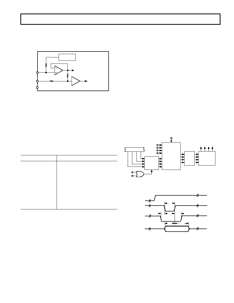
Figure 5 shows the arrangement used. The
H/S SEL controls a
multiplexer that selects the source of the conversion sequence
information, i.e., from the hardware channel select pins (SL1 to
SL4) or from the channel selection register. When a conversion
is started the output from the multiplexer is latched until the
end-of-the conversion sequence. The data bus bits DB0 to DB3
(DB0 representing Channel 1 through DB3 representing Chan-
nel 4) are bidirectional and become inputs to the channel select
register when
RD is logic high and CS and WR are logic low.
The logic state on DB0 to DB3 is latched into the channel select
register when
WR goes logic high. Figure 6 shows the loading
sequence for channel selection using software control. When
using software control to select the conversion sequence a write
is only required each time the conversion sequence needs
changing. This is because the channel select register will hold its
information until different information is written to it.
It should be noted that the hardware select Pins SL1 and SL2
are dual function. When
H/S SEL is logic high (selecting the
conversion sequence using software control) they take the func-
tions CLK IN and
INT/EXT CLK respectively. Therefore, the
logic inputs on these pins must be set according to the type of
operation required (see Using an External Clock). Also when
H/S SEL is high, the SL3 and SL4 logic inputs have no function
and can be tied either high or low, but should not be left floating.
DATA BUS
D0
D1
D2
D3
WR
CS
WR
CHANNEL
SELECT
REGISTER
SL1
SL2
SL3
SL4
HARDWARE CHANNEL
SELECT PINS
H/S
TRANSPARENT WHILE WAITING FOR
CONVST.
LATCHED ON THE RISING EDGE OF
CONVST AND
DURING A CONVERSION SEQUENCE.
MULTIPLEXER
LATCH
SEQUENCER
SELECT INDIVIDUAL
TRACK-AND-HOLDS
FOR CONVERSION
Figure 5. Channel Select Inputs and Registers
RD
WR
CS
DATA
t16
t17
t14
t15
DATA IN
t13
Figure 6. Channel Selection via Software Control
相关PDF资料 |
PDF描述 |
|---|---|
| AD7575BQ | IC ADC 8BIT LC2MOS W/HOLD 18CDIP |
| VE-BNZ-MV-F2 | CONVERTER MOD DC/DC 2V 60W |
| VE-260-CU-F3 | CONVERTER MOD DC/DC 5V 200W |
| MS27505E17F35P | CONN RCPT 55POS BOX MNT W/PINS |
| C6F | CONN RCPT FEMALE 6PIN |
相关代理商/技术参数 |
参数描述 |
|---|---|
| AD7865ASZ-3REEL-SCHNEIDER | 制造商:Analog Devices 功能描述: |
| AD7865BS-1 | 制造商:Rochester Electronics LLC 功能描述:4 CH. SIMULTANEOUS BIPOLAR,14-B ADC I.C. - Bulk 制造商:Analog Devices 功能描述:IC 14-BIT ADC |
| AD7865BS-1Z | 制造商:Analog Devices 功能描述:ADC 14BIT 4CH 350KSPS 44LQ 制造商:Analog Devices 功能描述:ADC, 14BIT, 4CH, 350KSPS, 44LQFP; Resolution (Bits):14bit; Sampling Rate:350kSPS; Supply Voltage Type:Single; Supply Voltage Min:4.75V; Supply Voltage Max:5.25V; Supply Current:32mA; Digital IC Case Style:LQFP; No. of Pins:44; Input ;RoHS Compliant: Yes |
| AD7865BS-2 | 制造商:Rochester Electronics LLC 功能描述:4 CH. SIMULTANEOUS BIPOLAR,14-B ADC I.C. - Bulk |
| AD7865BS-2REEL | 制造商:Analog Devices 功能描述:ADC Single SAR 350ksps 14-bit Parallel 44-Pin MQFP T/R |
发布紧急采购,3分钟左右您将得到回复。