- 您现在的位置:买卖IC网 > PDF目录10092 > AD7865YSZ-1 (Analog Devices Inc)IC ADC 14BIT 4CHAN 5V 44-MQFP PDF资料下载
参数资料
| 型号: | AD7865YSZ-1 |
| 厂商: | Analog Devices Inc |
| 文件页数: | 6/19页 |
| 文件大小: | 0K |
| 描述: | IC ADC 14BIT 4CHAN 5V 44-MQFP |
| 标准包装: | 1 |
| 位数: | 14 |
| 采样率(每秒): | 350k |
| 数据接口: | 并联 |
| 转换器数目: | 1 |
| 功率耗散(最大): | 160mW |
| 电压电源: | 模拟和数字 |
| 工作温度: | -40°C ~ 105°C |
| 安装类型: | 表面贴装 |
| 封装/外壳: | 44-QFP |
| 供应商设备封装: | 44-MQFP(10x10) |
| 包装: | 托盘 |
| 输入数目和类型: | 4 个差分,双极 |
REV. B
AD7865
–14–
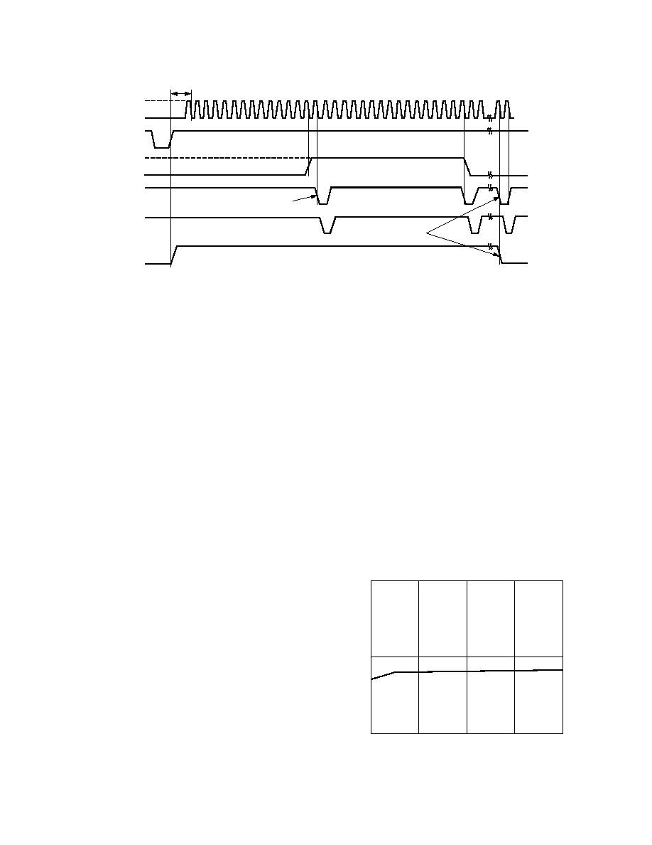
Using an External Clock
With the
H/S SEL and INT/EXT CLK pins tied to Logic 1, the
AD7865 will expect to be driven from an external clock. The
highest external clock frequency allowed is 5 MHz. This means
a conversion time of 3.2
s compared to 2.4 s using the inter-
nal clock. In some instances, however, it may be useful to use an
external clock when high throughput rates are not required. For
example, two or more AD7865s may be synchronized by using
the same external clock for all devices. In this way there is no
latency between output logic signals like
EOC due to differences
in the frequency of the internal clock oscillators. Figure 10
shows how the various logic outputs are synchronized to the CLK
signal. The first falling edge of CLKIN must not occur until
200 ns after a conversion has been initiated (rising edge of
CONVST), at which point BUSY will go high. The AD7865
will then convert the analog input signal on the first selected
channel (see Selecting a Conversion Sequence) at a rate deter-
mined by the CLKIN. No external events will occur until the
14th falling edge of CLKIN. The data register output address
is then reset to point to Data Register 1 and FRSTDATA goes
high. This first conversion is complete on the 15th falling edge
of the CLKIN (indicated by
EOC going low) and the result
from this conversion is loaded into Data Register 1.
EOC goes
high again on the 16th falling edge of CLKIN. Figure 10 shows
a
RD pulse occurring when EOC is low, enabling the conversion
result in Data Register 1 onto the data bus. The next 16 pulses
of CLKIN will convert the analog input signal on the second
selected channel and so on until all selected channels have been
converted. BUSY and
EOC will go low on the 15th falling edge
of the last conversion sequence and
EOC will return high on the
16th falling edge.
Standby Mode Operation
The AD7865 has a Standby Mode whereby the device can be
placed in a low current consumption mode (3
A typ). The
AD7865 is placed in standby by bringing the logic input
STBY
low. The AD7865 can be powered up again for normal opera-
tion by bringing
STBY logic high. The output data buffers are
still operational while the AD7865 is in standby. This means the
user can still continue to access the conversion results while the
AD7865 is in standby. This feature can be used to reduce the
average power consumption in a system using low throughput
rates. To reduce the average power consumption the AD7865 can
be placed in standby at the end of each conversion sequence,
i.e., when BUSY goes low and taken out of standby again prior
to the start of the next conversion sequence. The time it takes
the AD7865 to come out of standby is called the “wake-up”
time. This wake-up time will limit the maximum throughput
rate at which the AD7865 can be operated when powering down
between conversions. The AD7865 will wake up in less than
1
s when using an external reference. When the internal refer-
ence is used, the wake-up time depends on the amount of time
the AD7865 spends in standby mode. For standby times of less
than 10 ms the AD7865 will wake up in less than 5
s (see Fig-
ure 11). For standby times greater than this some or all of the
charge on the external reference capacitor will have leaked away
and the wake-up time will be dependent on how long it takes to
recharge. For standby times less than one second the wake-up
time will be less than 1 ms. Even if the charge has been completely
depleted the wake-up time will typically be less than 10 ms.
STANDBY TIME –
s
0
2500
5000
7500
10000
2.5
5
WAKE-UP
TIME
–
s
Figure 11. Wake-Up Time vs. Standby Time Using the On-
Chip Reference
FIRST CONVERSION
COMPLETE
BUSY
RD
EOC
FRSTDATA
CONVST
CLK
t18
2 34567 89 10 11 12 13 14 15 16 1
23456789 10 11 12 13 14
1
15 16
16
15
LAST CONVERSION
COMPLETE
Figure 10. Using an External Clock
相关PDF资料 |
PDF描述 |
|---|---|
| VE-JTV-MX-S | CONVERTER MOD DC/DC 5.8V 75W |
| VE-2NW-MX-F3 | CONVERTER MOD DC/DC 5.5V 75W |
| LTC1604CG#TRPBF | IC A/D CONV 16BIT SAMPLNG 36SSOP |
| IDT72215LB15PFI8 | IC FIFO 512X18 SYNC 15NS 64-TQFP |
| VI-2TY-MX | CONVERTER MOD DC/DC 3.3V 49.5W |
相关代理商/技术参数 |
参数描述 |
|---|---|
| AD7865YSZ-2 | 功能描述:IC ADC 14BIT 4CHAN 5V 44-MQFP RoHS:是 类别:集成电路 (IC) >> 数据采集 - 模数转换器 系列:- 标准包装:1 系列:- 位数:14 采样率(每秒):83k 数据接口:串行,并联 转换器数目:1 功率耗散(最大):95mW 电压电源:双 ± 工作温度:0°C ~ 70°C 安装类型:通孔 封装/外壳:28-DIP(0.600",15.24mm) 供应商设备封装:28-PDIP 包装:管件 输入数目和类型:1 个单端,双极 |
| AD7865YSZ-3 | 功能描述:IC ADC 14BIT 4CHAN 5V 44-MQFP RoHS:是 类别:集成电路 (IC) >> 数据采集 - 模数转换器 系列:- 标准包装:1 系列:- 位数:14 采样率(每秒):83k 数据接口:串行,并联 转换器数目:1 功率耗散(最大):95mW 电压电源:双 ± 工作温度:0°C ~ 70°C 安装类型:通孔 封装/外壳:28-DIP(0.600",15.24mm) 供应商设备封装:28-PDIP 包装:管件 输入数目和类型:1 个单端,双极 |
| AD7866 | 制造商:AD 制造商全称:Analog Devices 功能描述:Dual 1 MSPS, 12-Bit, 2-Channel SAR ADC with Serial Interface |
| AD7866ARU | 功能描述:IC ADC 12BIT 2CH DUAL 20-TSSOP RoHS:否 类别:集成电路 (IC) >> 数据采集 - 模数转换器 系列:- 标准包装:1,000 系列:- 位数:12 采样率(每秒):300k 数据接口:并联 转换器数目:1 功率耗散(最大):75mW 电压电源:单电源 工作温度:0°C ~ 70°C 安装类型:表面贴装 封装/外壳:24-SOIC(0.295",7.50mm 宽) 供应商设备封装:24-SOIC 包装:带卷 (TR) 输入数目和类型:1 个单端,单极;1 个单端,双极 |
| AD7866ARU-REEL | 制造商:Analog Devices 功能描述:ADC Dual SAR 1Msps 12-bit Serial 20-Pin TSSOP T/R |
发布紧急采购,3分钟左右您将得到回复。