- 您现在的位置:买卖IC网 > PDF目录1984 > AD7866ARU-REEL7 (Analog Devices Inc)IC ADC 12BIT 2CH DUAL 20TSSOP PDF资料下载
参数资料
| 型号: | AD7866ARU-REEL7 |
| 厂商: | Analog Devices Inc |
| 文件页数: | 13/24页 |
| 文件大小: | 0K |
| 描述: | IC ADC 12BIT 2CH DUAL 20TSSOP |
| 产品变化通告: | Product Discontinuance 27/Oct/2011 |
| 标准包装: | 1,000 |
| 位数: | 12 |
| 采样率(每秒): | 1M |
| 数据接口: | DSP,MICROWIRE?,QSPI?,串行,SPI? |
| 转换器数目: | 2 |
| 功率耗散(最大): | 24mW |
| 电压电源: | 模拟和数字 |
| 工作温度: | -40°C ~ 125°C |
| 安装类型: | 表面贴装 |
| 封装/外壳: | 20-TSSOP(0.173",4.40mm 宽) |
| 供应商设备封装: | 20-TSSOP |
| 包装: | 带卷 (TR) |
| 输入数目和类型: | 4 个单端,单极 |
| 配用: | EVAL-AD7866CBZ-ND - BOARD EVALUATION AD7866 |
REV. A
–20–
AD7866
For example, if the ADSP-2189 had a 20 MHz crystal such that it
had a master clock frequency of 40 MHz, then the master cycle
time would be 25 ns. If the SCLKDIV register is loaded with the
value 3, an SCLK of 5 MHz is obtained and eight master clock
periods will elapse for every 1 SCLK period. Depending on the
throughput rate selected, if the timer register were loaded with the
value, 803, (803 + 1 = 804), for example, 100.5 SCLKs would
occur between interrupts and subsequently between transmit
instructions. This situation would result in nonequidistant
sampling as the transmit instruction is occurring on an SCLK
edge. If the number of SCLKs between interrupts were a whole
integer figure of N, equidistant sampling would be implemented
by the DSP.
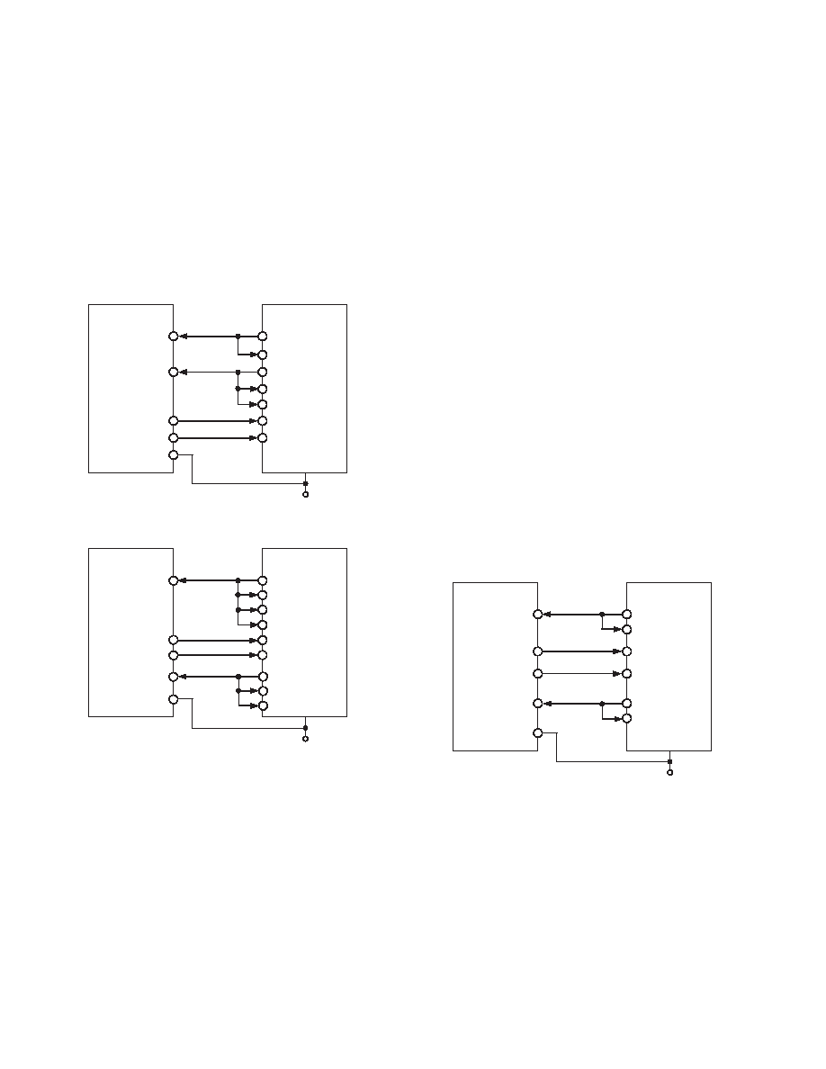
AD7866*
VDRIVE
DOUTA
DOUTB
CS
SCLK
ADSP-218x*
DR0
DR1
TFS0
SCLK0
RFS0
RSF1
SCLK1
*ADDITIONAL PINS OMITTED
FOR CLARITY
VDD
Figure 24. Interfacing the AD7866 to the ADSP-218x
AD7866*
VDRIVE
DOUTA
DOUTB
CS
SCLK
TMS320C541*
DR0
DR1
CLKX0
CLKR0
CLKX1
CLKR1
*ADDITIONAL PINS OMITTED
FOR CLARITY
VDD
FSX0
FSR0
FSR1
Figure 25. Interfacing the AD7866 to the TMS320C541
AD7866 to TMS320C541
The serial interface on the TMS320C541 uses a continuous serial
clock and frame synchronization signals to synchronize the data
transfer operations with peripheral devices like the AD7866. The
CS input allows easy interfacing between the TMS320C541 and
the AD7866 with no glue logic required. The serial ports of
the TMS320C541 are set up to operate in burst mode with internal
CLKX (Tx serial clock on serial port 0) and FSX0 (Tx frame sync
from serial port 0). The serial port control (SPC) registers must have
the following setup:
SPC0: FO = 0, FSM = 1, MCM = 1 and TxM = 1
SPC1: FO = 0, FSM = 1, MCM = 0 and TxM = 0
The format bit, FO, may be set to 1 to set the word length to
eight bits, in order to implement the power-down modes on the AD7866.
The connection diagram is shown in Figure 25. It should be noted
that for signal processing applications, it is imperative that the
frame synchronization signal from the TMS320C541 will provide
equidistant sampling. The VDRIVE pin of the AD7866 takes the
same supply voltage as that of the TMS320C541. This allows the
ADC to operate at a higher voltage than the serial interface, i.e.,
TMS320C541, if necessary.
AD7866 to DSP-563xx
The connection diagram in Figure 26 shows how the AD7866
can be connected to the ESSI (synchronous serial interface) of
the DSP-563xx family of DSPs from Motorola. Each ESSI
(there are two on-board) is operated in synchronous mode
(bit SYN = 1 in CRB register) with internally generated word
length frame sync for both Tx and Rx (bits FSL1 = 0 and FSL0 = 0
in CRB). Normal operation of the ESSI is selected by making
MOD = 0 in the CRB. Set the word length to 16 by setting bits
WL1 = 1 and WL0 = 0 in CRA. To implement the power-down
modes on the AD7866, the word length can be changed to eight
bits by setting bits WL1 = 0 and WL0 = 0 in CRA. The FSP bit
in the CRB should be set to 1 to make the frame sync negative.
It should be noted that for signal processing applications, it is
imperative that the frame synchronization signal from the
DSP-563xx provide equidistant sampling.
In the example shown in Figure 26, the serial clock is taken from
the ESSI0, so the SCK0 pin must be set as an output, SCKD = 1,
while the SCK1 pin is set up as an input, SCKD = 0. The frame
sync signal is taken from SC02 on ESSI0, so SCD2 = 1, while
on ESSI1, SCD2 = 0, so SC12 is configured as an input. The
VDRIVE pin of the AD7866 takes the same supply voltage as that
of the DSP-563xx. This allows the ADC to operate at a higher
voltage than the serial interface, i.e., DSP-563xx, if necessary.
AD7866*
VDRIVE
DOUTA
DOUTB
CS
SCLK
DSP-563xx*
SC02
SC12
SCK0
SRD0
SRD1
SCK1
*ADDITIONAL PINS OMITTED
FOR CLARITY
VDD
Figure 26. Interfacing to the DSP-563xx
APPLICATION HINTS
Grounding and Layout
The analog and digital supplies to the AD7866 are independent
and separately pinned out to minimize coupling between the analog
and digital sections of the device. The AD7866 has very good
immunity to noise on the power supplies as can be shown by the
PSRR vs. Supply Ripple Frequency plots, TPC 3a to TPC 4b.
However, care should be taken with regard to grounding and
layout.
The printed circuit board that houses the AD7866 should be
designed such that the analog and digital sections are separated
and confined to certain areas of the board. This facilitates the
use of ground planes that can be easily separated. A minimum
相关PDF资料 |
PDF描述 |
|---|---|
| AD7871KP | IC ADC 14BIT SAMPLING 28-PLCC |
| AD7873ARUZ | IC ADC 12BIT TOUCHSCREEN 16TSSOP |
| AD7875LNZ | IC ADC 12BIT SAMPLING 5V 24-DIP |
| AD7877WACPZ-REEL7 | IC CTRLR TOUCH SCREEN 32LFCSP |
| AD7878KPZ | IC ADC 12BIT W/DSP INT 28-PLCC |
相关代理商/技术参数 |
参数描述 |
|---|---|
| AD7866ARUZ | 功能描述:IC ADC 12BIT 2CH DUAL 20-TSSOP RoHS:是 类别:集成电路 (IC) >> 数据采集 - 模数转换器 系列:- 标准包装:1 系列:microPOWER™ 位数:8 采样率(每秒):1M 数据接口:串行,SPI? 转换器数目:1 功率耗散(最大):- 电压电源:模拟和数字 工作温度:-40°C ~ 125°C 安装类型:表面贴装 封装/外壳:24-VFQFN 裸露焊盘 供应商设备封装:24-VQFN 裸露焊盘(4x4) 包装:Digi-Reel® 输入数目和类型:8 个单端,单极 产品目录页面:892 (CN2011-ZH PDF) 其它名称:296-25851-6 |
| AD7866ARUZ-REEL | 功能描述:IC ADC 12BIT 2CHAN DUAL 20TSSOP RoHS:是 类别:集成电路 (IC) >> 数据采集 - 模数转换器 系列:- 标准包装:1,000 系列:- 位数:16 采样率(每秒):45k 数据接口:串行 转换器数目:2 功率耗散(最大):315mW 电压电源:模拟和数字 工作温度:0°C ~ 70°C 安装类型:表面贴装 封装/外壳:28-SOIC(0.295",7.50mm 宽) 供应商设备封装:28-SOIC W 包装:带卷 (TR) 输入数目和类型:2 个单端,单极 |
| AD7866ARUZ-REEL7 | 功能描述:IC ADC 12BIT 2CHAN DUAL 20TSSOP RoHS:是 类别:集成电路 (IC) >> 数据采集 - 模数转换器 系列:- 标准包装:1,000 系列:- 位数:16 采样率(每秒):45k 数据接口:串行 转换器数目:2 功率耗散(最大):315mW 电压电源:模拟和数字 工作温度:0°C ~ 70°C 安装类型:表面贴装 封装/外壳:28-SOIC(0.295",7.50mm 宽) 供应商设备封装:28-SOIC W 包装:带卷 (TR) 输入数目和类型:2 个单端,单极 |
| AD7866BRU | 功能描述:IC ADC 12BIT 2CH DUAL 20-TSSOP RoHS:否 类别:集成电路 (IC) >> 数据采集 - 模数转换器 系列:- 标准包装:1,000 系列:- 位数:12 采样率(每秒):300k 数据接口:并联 转换器数目:1 功率耗散(最大):75mW 电压电源:单电源 工作温度:0°C ~ 70°C 安装类型:表面贴装 封装/外壳:24-SOIC(0.295",7.50mm 宽) 供应商设备封装:24-SOIC 包装:带卷 (TR) 输入数目和类型:1 个单端,单极;1 个单端,双极 |
| AD7866BRU-REEL | 制造商:Analog Devices 功能描述:ADC Dual SAR 1Msps 12-bit Serial 20-Pin TSSOP T/R |
发布紧急采购,3分钟左右您将得到回复。