参数资料
| 型号: | AD7868BNZ |
| 厂商: | Analog Devices Inc |
| 文件页数: | 3/16页 |
| 文件大小: | 0K |
| 描述: | IC I/O PORT 12BIT ANLG 24-DIP |
| 产品变化通告: | AD7868 Discontinuation 05/Sept/2011 |
| 标准包装: | 1 |
| 应用: | 模拟 I/O |
| 接口: | TTL/CMOS |
| 电源电压: | 4.75 V ~ 5.25 V |
| 封装/外壳: | 24-DIP(0.300",7.62mm) |
| 供应商设备封装: | 24-PDIP |
| 包装: | 管件 |
| 安装类型: | 通孔 |
AD7868
–11–
REV. B
MICROPROCESSOR INTERFACING
Microprocessor interfacing to the AD7868 is via a serial bus that
uses standard protocol compatible with DSP machines. The
communication interface consists of separate transmit (DAC)
and receive (ADC) sections whose operations can be either syn-
chronous or asynchronous with respect to each other. Each sec-
tion has a clock signal, a data signal and a frame or strobe pulse.
Synchronous operation means that data is transmitted from the
ADC and to the DAC at the same time. In this mode only one
interface clock is needed and this has to be the ADC clock out,
so RCLK must be connected to TCLK. For asynchronous op-
eration, DAC and ADC data transfers are independent of each
other, the ADC provides the receive clock (RCLK) while the
transmit clock (TCLK) may be provided by the processor or the
ADC or some other external clock source.
Another option to be considered with serial interfacing is the use
of a gated clock. A gated clock means that the device that is
sending the data switches on the clock when data is ready to be
transmitted and three states the clock output when transmission
is complete. Only 16 clock pulses are transmitted with the first
data bit getting latched into the receiving device on the first fall-
ing clock edge. Ideally, there is no need for frame pulses, how-
ever, the AD7868 DAC frame input (TFS) has to be driven
high between data transmissions. The easiest method is to use
RFS
to drive TFS and use only synchronous interfacing. This
avoids the use of interconnects between the processor and
AD7868 frame signals. Not all processors have a gated clock
facility, Figure 16 shows an example with the DSP56000.
Table I below shows the number of interconnect lines between
the processor and the AD7868 for the different interfacing op-
tions. The AD7868 has the facility to use different clocks for
transmitting and receiving data. This option, however, only ex-
ists on some processors and normally just one clock (ADC
clock) is used for all communication with the AD7868. For sim-
plicity, all the interface examples in this data sheet use synchro-
nous interfacing and use the ADC clock (RCLK) as an input for
the DAC clock (TCLK). For a better understanding of each of
these interfaces, consult the relevant processor data sheet.
Table I. Interconnect Lines for Different Interfacing Options
No. of
Configuration
Interconnects
Signals
Synchronous
4
RCLK, DR, DT and RFS
(TCLK = RCLK, TFS = RFS)
Asynchronous*
5 or 6
RCLK, DR, RFS, DT, TFS
(TCLK = RCLK or
P serial CLK)
Synchronous
3
RCLK, DR and DT
Gated Clock
(TCLK = RCLK, TFS = RFS)
*5 LINES OF INTERCONNECT WHEN TCLK = RCLK
6 LINES OF INTERCONNECT WHEN TCLK =
P SERIAL CLK
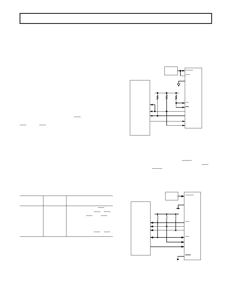
AD7868—DSP56000 Interface
Figure 16 shows a typical interface between the AD7868 and
DSP56000. The interface arrangement is synchronous with a
gated clock requiring only three lines of interconnect. The
DSP56000 internal serial control registers have to be configured
for a 16-bit data word with valid data on the first falling clock
edge. Conversion starts and DAC updating are controlled by an
external timer. Data transfers, which occur during ADC conver-
sions, are between the processor receive and transmit shift regis-
ters and the AD7868’s ADC and DAC. At the end of each
16-bit transfer the DSP56000 receives an internal interrupt indi-
cating the transmit register is empty and the receive register is
full.
DSP56000
STD
TFS
*ADDITIONAL PINS OMITTED FOR CLARITY
DT
SCK
SRD
RCLK
DR
CONVST
RFS
TIMER
AD7868*
4.7k
2k
4.7k
LDAC
CONTROL
TCLK
5V
+
SC0
Figure 16. AD7868—DSP56000 Interface
AD7868—ADSP-2101/ADSP-2102 Interface
An interface which is suitable for the ADSP-2101 or the ADSP-
2102 is shown in Figure 17. The interface is configured for syn-
chronous, continuous clock operation. The LDAC is tied low so
the DAC gets updated on the sixteenth falling clock after TFS
goes low. Alternatively LDAC may be driven from a timer as
shown in Figure 16. As with the previous interface the processor
receives an interrupt after reading or writing to the AD7868 and
updates its own internal registers in preparation for the next
data transfer.
ADSP-2101/
ADSP-2102
TFS
DT
TCLK
DT
LDAC
TFS
*ADDITIONAL PINS OMITTED FOR CLARITY
RFS
SCLK
DR
RCLK
DR
CONVST
RFS
CONTROL
TIMER
AD7868*
4.7k
2k
4.7k
5V
–
5V
+
Figure 17. AD7868—ADSP-2101/ADSP-2102 Interface
相关PDF资料 |
PDF描述 |
|---|---|
| AD7869JRZ | IC I/O PORT 14BIT ANLG 28SOIC |
| AD7874SE | IC DAS 12BIT 4CH 5V 28-CLCC |
| AD7890BRZ-4 | IC DAS 12BIT 8CH 24-SOIC |
| AD7891BPZ-2 | IC DAS 12BIT 8CH 44-PLCC |
| AD80066KRSZRL | IC DSP CTLR 16BIT 28SSOP |
相关代理商/技术参数 |
参数描述 |
|---|---|
| AD7868BQ | 制造商:Rochester Electronics LLC 功能描述:- Bulk |
| AD7868BR | 制造商:Analog Devices 功能描述:Data Acquisition System Single ADC Single DAC 12-Bit 28-Pin SOIC W 制造商:Rochester Electronics LLC 功能描述:ANALOG I/O PORT IC - Bulk |
| AD7868BR-REEL | 功能描述:IC I/O PORT 12BIT ANLG 28-SOIC RoHS:否 类别:集成电路 (IC) >> 接口 - 专用 系列:- 标准包装:3,000 系列:- 应用:PDA,便携式音频/视频,智能电话 接口:I²C,2 线串口 电源电压:1.65 V ~ 3.6 V 封装/外壳:24-WQFN 裸露焊盘 供应商设备封装:24-QFN 裸露焊盘(4x4) 包装:带卷 (TR) 安装类型:表面贴装 产品目录页面:1015 (CN2011-ZH PDF) 其它名称:296-25223-2 |
| AD7868BRZ | 功能描述:IC I/O PORT 12BIT ANLG 28SOIC RoHS:是 类别:集成电路 (IC) >> 接口 - 专用 系列:- 标准包装:3,000 系列:- 应用:PDA,便携式音频/视频,智能电话 接口:I²C,2 线串口 电源电压:1.65 V ~ 3.6 V 封装/外壳:24-WQFN 裸露焊盘 供应商设备封装:24-QFN 裸露焊盘(4x4) 包装:带卷 (TR) 安装类型:表面贴装 产品目录页面:1015 (CN2011-ZH PDF) 其它名称:296-25223-2 |
| AD7868BRZ-REEL | 功能描述:IC I/O PORT 12BIT ANLG 28SOIC RoHS:是 类别:集成电路 (IC) >> 接口 - 专用 系列:- 标准包装:3,000 系列:- 应用:PDA,便携式音频/视频,智能电话 接口:I²C,2 线串口 电源电压:1.65 V ~ 3.6 V 封装/外壳:24-WQFN 裸露焊盘 供应商设备封装:24-QFN 裸露焊盘(4x4) 包装:带卷 (TR) 安装类型:表面贴装 产品目录页面:1015 (CN2011-ZH PDF) 其它名称:296-25223-2 |
发布紧急采购,3分钟左右您将得到回复。