- 您现在的位置:买卖IC网 > PDF目录11786 > AD7869JNZ (Analog Devices Inc)IC I/O PORT 14BIT ANLG 24DIP PDF资料下载
参数资料
| 型号: | AD7869JNZ |
| 厂商: | Analog Devices Inc |
| 文件页数: | 12/16页 |
| 文件大小: | 0K |
| 描述: | IC I/O PORT 14BIT ANLG 24DIP |
| 标准包装: | 1 |
| 应用: | 模拟 I/O |
| 接口: | TTL/CMOS |
| 电源电压: | 4.75 V ~ 5.25 V |
| 封装/外壳: | 24-DIP(0.300",7.62mm) |
| 供应商设备封装: | 24-PDIP |
| 包装: | 管件 |
| 安装类型: | 通孔 |
AD7869
–5–
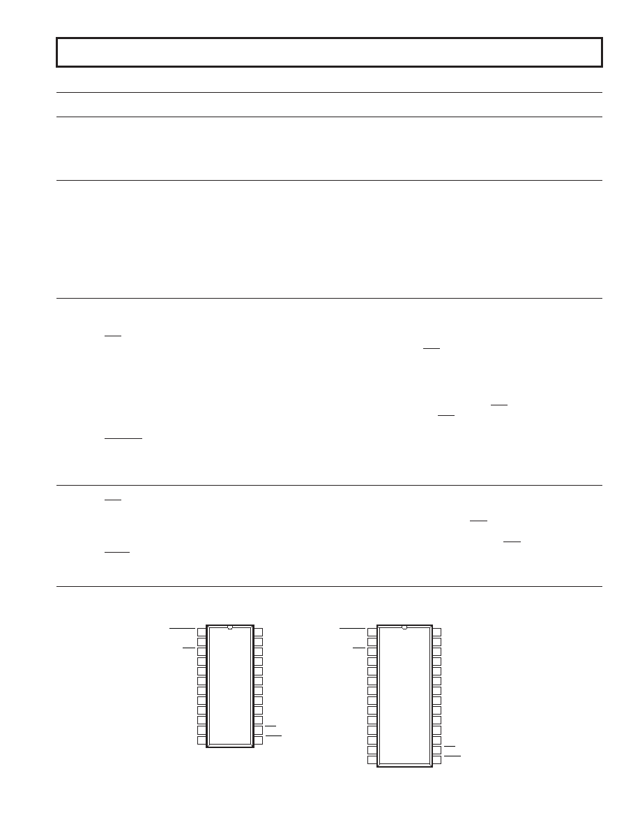
AD7869 PIN FUNCTION DESCRIPTION
DIP Pin
Number
Mnemonic
Function
POWER SUPPLY
7 & 23
VDD
Positive Power Supply, 5 V
± 5%. Both VDD pins must be tied together.
10 & 22
VSS
Negative Power Supply, –5 V
± 5%. Both VSS pins must be tied together.
8 & 19
AGND
Analog Ground. Both AGND pins must be tied together.
6 & 17
DGND
Digital Ground. Both DGND pins must be tied together.
ANALOG SIGNAL AND REFERENCE
21
VIN
ADC Analog Input. The ADC input range is
±3 V.
9VOUT
Analog Output Voltage from DAC. This output comes from a buffer amplifier. The range is bipolar,
±3 V
with RI DAC = +3 V.
20
RO ADC
Voltage Reference Output. The internal ADC 3 V reference is provided at this pin. This output may be used as a
reference for the DAC by connecting it to the RI DAC input. The external load capability of this reference is 500
μA.
11
RO DAC
DAC Voltage Reference Output. This is one of two internal voltage references. To operate the DAC with this
internal reference, RO DAC should be connected to RI DAC. The external load capability of the reference is 500
μA.
12
RI DAC
DAC Voltage Reference Input. The voltage reference for the DAC must be applied to this pin. It is internally
buffered before being applied to the DAC. The nominal reference voltage for correct operation of the AD7869 is 3 V.
ADC INTERFACE AND CONTROL
2
CLK
Clock Input. An external TTL-compatible clock may be applied to this input. Alternatively, tying this pin to VSS
enables the internal laser-trimmed oscillator.
3
RFS
Receive Frame Synchronization, Logic Output. This is an active low open-drain output that provides a framing
pulse for serial data. An external 4.7 k
Ω pull-up resistor is required on RFS.
4
RCLK
Receive Clock, Logic Output. RCLK is the gated serial clock output that is derived from the internal or external
ADC clock. If the CONTROL input is at VSS, the clock runs continuously. With the CONTROL input at DGND,
the RCLK output is gated off (three-state) after serial transmission is complete. RCLK is an open-drain output and
requires an external 2 k
Ω pull-up resistor.
5
DR
Receive Data, Logic Output. This is an open-drain data output used in conjunction with
RFS and RCLK to transmit
data from the ADC. Serial data is valid on the falling edge of RCLK when
RFS is low. An external 4.7 kΩ resistor is
required on the DR output.
1
CONVST
Convert Start, Logic Input. A low to high transition on this input puts the track-and-hold amplifier into the hold
mode and starts an ADC conversion. This input is asynchronous to the CLK input.
24
CONTROL
Control, Logic Input. With this pin at 0 V, the RCLK is noncontinuous. With this pin at –5 V, the RCLK is contin-
uous. Note, tying this pin to VDD places the part in a factory test mode where normal operation is not exhibited.
DAC INTERFACE AND CONTROL
14
TFS
Transmit Frame Synchronization, Logic Input. This is a frame or synchronization signal for the DAC with serial
data expected after the falling edge of this signal.
15
DT
Transmit Data, Logic Input. This is the data input that is used in conjunction with
TFS and TCLK to transfer
serial data to the input latch.
16
TCLK
Transmit Clock, Logic Input. Serial data bits are latched on the falling edge of TCLK when
TFS is low.
13
LDAC
Load DAC, Logic Input. A new word is transferred into the DAC latch from the input latch on the falling edge
of this signal.
18
NC
No Connect.
REV. B
CONVST
1
CLK
2
RFS
3
RCLK
4
CONTROL
24
VDD
23
VSS
22
VIN
21
DR
5
DGND
6
VDD 7
RO ADC
20
AGND
19
NC
18
AGND
8
DGND
17
VOUT 9
TCLK
16
VSS 10
DT
15
RO DAC 11
TFS
14
RI DAC 12
LDAC
13
NC = NO CONNECT
AD7869
TOP VIEW
(Not to Scale)
AD7869
TOP VIEW
(Not to Scale)
CONVST
1
CLK
2
RFS
3
NC
4
RCLK
5
DR
6
DGND
7
VDD 8
AGND
9
VOUT 10
VSS 12
CONTROL
28
VDD
27
VSS
26
NC
25
VIN
24
RO ADC
23
AGND
22
DGND
21
TCLK
20
NC
19
NC 11
NC
18
RO DAC 13
TFS
16
RI DAC 14
LDAC
15
DT
17
NC = NO CONNECT
DIP
SOIC
PIN CONFIGURATIONS
相关PDF资料 |
PDF描述 |
|---|---|
| AD6641BCPZ-500 | IC IF RCVR 11BIT 200MSPS 56LFCSP |
| VI-JTJ-IW-F3 | CONVERTER MOD DC/DC 36V 100W |
| VI-JTJ-IW-F2 | CONVERTER MOD DC/DC 36V 100W |
| 1604037-4 | CONN HOUSING POWER 2POLE BATTERY |
| VI-JTH-IW-F4 | CONVERTER MOD DC/DC 52V 100W |
相关代理商/技术参数 |
参数描述 |
|---|---|
| AD7869JQ | 制造商:Rochester Electronics LLC 功能描述:- Bulk |
| AD7869JR | 制造商:Analog Devices 功能描述:Data Acquisition System Single ADC Single DAC 14-Bit 28-Pin SOIC W 制造商:Analog Devices 功能描述:DATA ACQ SYS SGL ADC SGL DAC 14BIT 28SOIC W - Rail/Tube |
| AD7869JRZ | 功能描述:IC I/O PORT 14BIT ANLG 28SOIC RoHS:是 类别:集成电路 (IC) >> 接口 - 专用 系列:- 特色产品:NXP - I2C Interface 标准包装:1 系列:- 应用:2 通道 I²C 多路复用器 接口:I²C,SM 总线 电源电压:2.3 V ~ 5.5 V 封装/外壳:16-TSSOP(0.173",4.40mm 宽) 供应商设备封装:16-TSSOP 包装:剪切带 (CT) 安装类型:表面贴装 产品目录页面:825 (CN2011-ZH PDF) 其它名称:568-1854-1 |
| AD7870 | 制造商:AD 制造商全称:Analog Devices 功能描述:LC2MOS Complete, 12-Bit, 100 kHz, Sampling ADCs |
| AD7870A | 制造商:AD 制造商全称:Analog Devices 功能描述:LC2MOS Complete, 12-Bit, 100 kHz , Sampling ADC |
发布紧急采购,3分钟左右您将得到回复。