- 您现在的位置:买卖IC网 > PDF目录10062 > AD7870KPZ (Analog Devices Inc)IC ADC 12BIT SAMPLING 3V 28PLCC PDF资料下载
参数资料
| 型号: | AD7870KPZ |
| 厂商: | Analog Devices Inc |
| 文件页数: | 4/28页 |
| 文件大小: | 0K |
| 描述: | IC ADC 12BIT SAMPLING 3V 28PLCC |
| 标准包装: | 1 |
| 位数: | 12 |
| 采样率(每秒): | 100k |
| 数据接口: | 串行,并联 |
| 转换器数目: | 1 |
| 功率耗散(最大): | 95mW |
| 电压电源: | 双 ± |
| 工作温度: | 0°C ~ 70°C |
| 安装类型: | 表面贴装 |
| 封装/外壳: | 28-LCC(J 形引线) |
| 供应商设备封装: | 28-PLCC(11.51x11.51) |
| 包装: | 管件 |
| 输入数目和类型: | 1 个单端,双极 |
第1页第2页第3页当前第4页第5页第6页第7页第8页第9页第10页第11页第12页第13页第14页第15页第16页第17页第18页第19页第20页第21页第22页第23页第24页第25页第26页第27页第28页
AD7870/AD7875/AD7876
Rev. C | Page 12 of 2
8
AD7876
TRACK-AND-HOLD
AMPLIFIER
TO INTERNAL
REFERENCE
2.1R
7R
VIN
REF OUT
AGND
TO INTERNAL
COMPARATOR
07
73
0-
00
9
3R
TO INTERNAL AGND
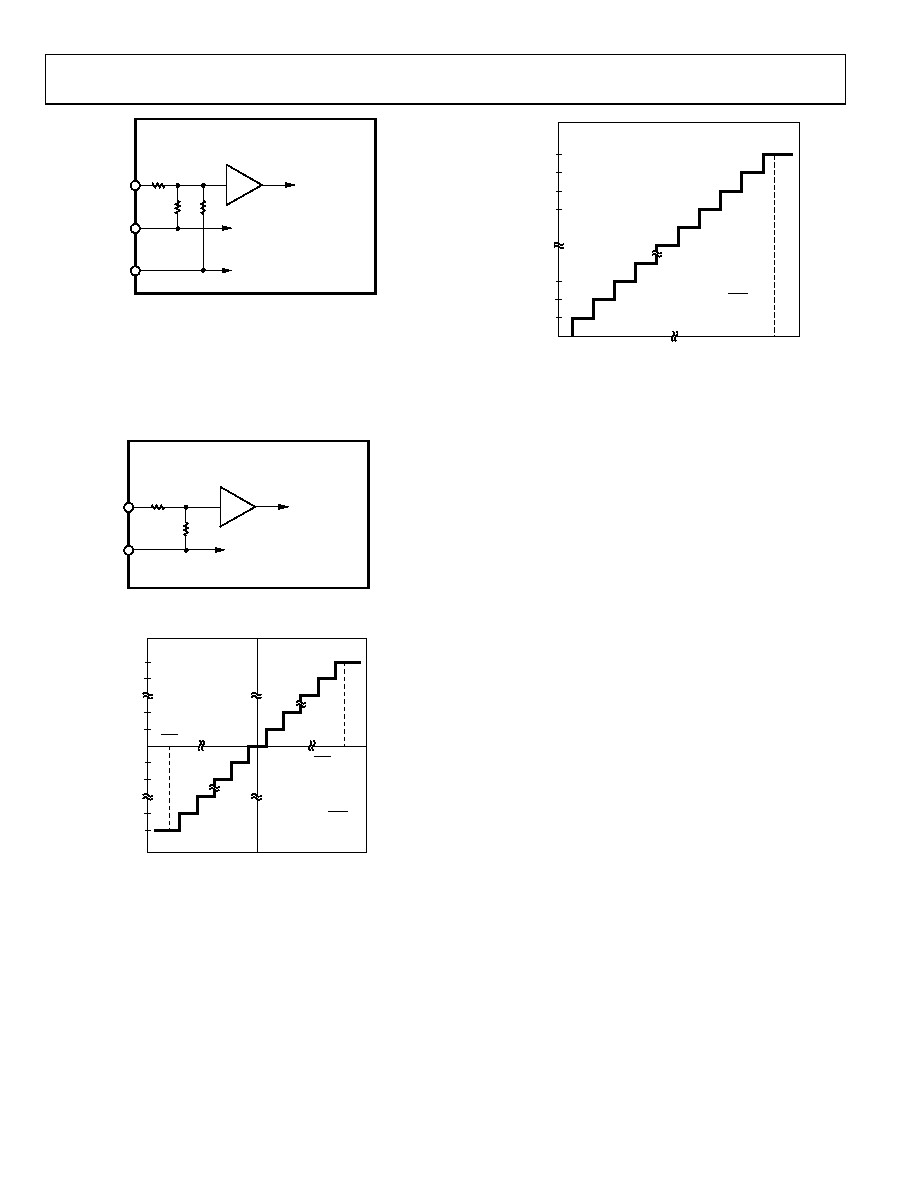
Figure 9. AD7876 Analog Input
Figure 10 shows the analog input for the AD7875. The input
range is 0 V to +5 V into an input resistance of typically 25 kΩ.
Once again, the designed code transitions occur midway
between successive integer LSB values. The output code is
straight binary with 1 LSB = FS/4096 = 5 V/4096 = 1.22 mV.
The ideal input/output transfer function is shown in Figure 12.
AD7875
TRACK-AND-HOLD
AMPLIFIER
TO INTERNAL AGND
3R
2R
VIN
AGND
TO INTERNAL
COMPARATOR
07
73
0-
01
0
Figure 10. AD7875 Analog Input
011…111
OUTPUT
CODE
AD7870 (AD7876)
011…110
100…001
100…000
0V
VIN – INPUT VOLTAGE
000…010
000…001
000…000
111…111
111…110
–FS
2
+FS – 1LSB
2
FS
1LSB =
FS = 6V (20V)
4096
07
73
0-
0
1
Figure 11. AD7870/AD7876 Transfer Function
OUTPUT
CODE
000…011
000…010
000…001
000…000
VIN – INPUT VOLTAGE
111…101
111…100
111…111
111…110
FS
1LSB =
FS = 5V
+FS – 1LSB
0V
4096
07
73
0-
0
12
Figure 12. AD7875 Transfer Function
OFFSET AND FULL-SCALE ADJUSTMENT—
AD7870
In most digital signal processing (DSP) applications, offset and
full-scale errors have little or no effect on system performance.
Offset error can always be eliminated in the analog domain
by ac coupling. Full-scale error effect is linear and does not
cause problems as long as the input signal is within the full
dynamic range of the ADC. Some applications will require
that the input signal span the full analog input dynamic range.
In such applications, offset and full-scale error have to be
adjusted to zero.
Where adjustment is required, offset error must be adjusted
before full-scale error. This is achieved by trimming the offset
of the op amp driving the analog input of the AD7870 while the
input voltage is 1/2 LSB below ground. The trim procedure is as
and adjust the op amp offset voltage until the ADC output code
flickers between 1111 1111 1111 and 0000 0000 0000. Gain
error can be adjusted at either the first code transition (ADC
negative full-scale) or the last code transition (ADC positive full
scale). The trim procedures for both cases are as follows (see
相关PDF资料 |
PDF描述 |
|---|---|
| VI-2N0-IW-F4 | CONVERTER MOD DC/DC 5V 100W |
| VI-2N0-IW-F3 | CONVERTER MOD DC/DC 5V 100W |
| VI-2N0-IW-F1 | CONVERTER MOD DC/DC 5V 100W |
| AD774BAR | IC ADC 12BIT W/BUFF REF 28-SOIC |
| IDT72V215L15PFI | IC FIFO SYNC 512X18 15NS 64-TQFP |
相关代理商/技术参数 |
参数描述 |
|---|---|
| AD7870KPZ1 | 制造商:AD 制造商全称:Analog Devices 功能描述:LC2MOS Complete, 12-Bit, 100 kHz, Sampling ADCs |
| AD7870KPZ-REEL | 功能描述:IC ADC 12BIT SAMPLING 3V 28PLCC RoHS:是 类别:集成电路 (IC) >> 数据采集 - 模数转换器 系列:- 标准包装:1 系列:- 位数:14 采样率(每秒):83k 数据接口:串行,并联 转换器数目:1 功率耗散(最大):95mW 电压电源:双 ± 工作温度:0°C ~ 70°C 安装类型:通孔 封装/外壳:28-DIP(0.600",15.24mm) 供应商设备封装:28-PDIP 包装:管件 输入数目和类型:1 个单端,双极 |
| AD7870KPZ-REEL1 | 制造商:AD 制造商全称:Analog Devices 功能描述:LC2MOS Complete, 12-Bit, 100 kHz, Sampling ADCs |
| AD7870LN | 制造商:AD 制造商全称:Analog Devices 功能描述:LC2MOS Complete, 12-Bit, 100 kHz, Sampling ADCs |
| AD7870LNZ | 功能描述:IC ADC 12BIT SAMPLING 3V 24-DIP RoHS:是 类别:集成电路 (IC) >> 数据采集 - 模数转换器 系列:- 标准包装:1 系列:- 位数:14 采样率(每秒):83k 数据接口:串行,并联 转换器数目:1 功率耗散(最大):95mW 电压电源:双 ± 工作温度:0°C ~ 70°C 安装类型:通孔 封装/外壳:28-DIP(0.600",15.24mm) 供应商设备封装:28-PDIP 包装:管件 输入数目和类型:1 个单端,双极 |
发布紧急采购,3分钟左右您将得到回复。