- 您现在的位置:买卖IC网 > PDF目录10047 > AD7870LPZ (Analog Devices Inc)IC ADC 12BIT SAMPLING 3V 28-PLCC PDF资料下载
参数资料
| 型号: | AD7870LPZ |
| 厂商: | Analog Devices Inc |
| 文件页数: | 7/28页 |
| 文件大小: | 0K |
| 描述: | IC ADC 12BIT SAMPLING 3V 28-PLCC |
| 产品变化通告: | Conversion Time Change |
| 标准包装: | 1 |
| 位数: | 12 |
| 采样率(每秒): | 100k |
| 数据接口: | 串行,并联 |
| 转换器数目: | 1 |
| 功率耗散(最大): | 95mW |
| 电压电源: | 双 ± |
| 工作温度: | 0°C ~ 70°C |
| 安装类型: | 表面贴装 |
| 封装/外壳: | 28-LCC(J 形引线) |
| 供应商设备封装: | 28-PLCC(11.51x11.51) |
| 包装: | 管件 |
| 输入数目和类型: | 1 个单端,双极 |
第1页第2页第3页第4页第5页第6页当前第7页第8页第9页第10页第11页第12页第13页第14页第15页第16页第17页第18页第19页第20页第21页第22页第23页第24页第25页第26页第27页第28页
AD7870/AD7875/AD7876
Rev. C | Page 15 of
28
CONVST
TRACK-AND-HOLD
GOES INTO HOLD
TRACK-AND-HOLD RETURNS
TO TRACK AND
ACQUISITION TIME BEGINS
THREE-STATE
VALID
DATA
DB11 TO DB0
CS
RD
INT
DATA
t2
t1
tCONVERT
t5
t4
t7
t4
t3
07
73
0-
01
4
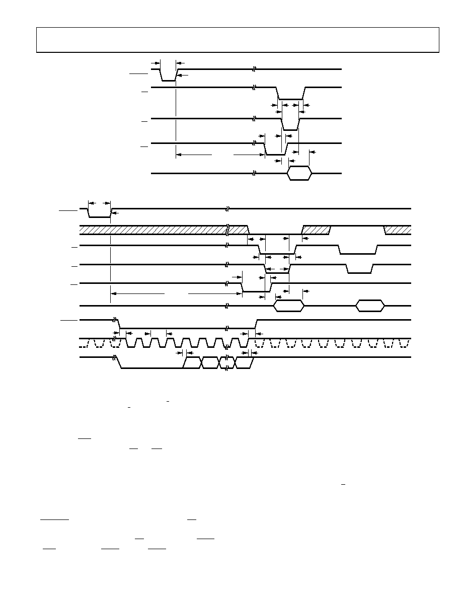
Figure 14. Mode 1 Timing Diagram, 12-Bit Parallel Read
CONVST
CS
RD
INT
SSTRB2
DATA
SCLK3
TRACK-AND-HOLD RETURNS TO TRACK
AND ACQUISITION TIME BEGINS
TRACK-AND-HOLD GOES INTO HOLD
THREE-STATE
LEADING
ZEROS
VALID
DATA
DB7 TO DB0
VALID
DATA
DB11 TO DB8
HBEN1
t1
SDATA2
1TIMES
t2, t3, t4, t8, AND t9 ARE THE SAME FOR A HIGH BYTE READ AS FOR A LOW BYTE READ.
2EXTERNAL 4.7k PULL-UP RESISTOR.
3EXTERNAL 2k PULL-UP RESISTOR;
CONTINUOUS SCLK (DASHED LINE) WHEN 12/8/CLK = –5V;
NONCONTINUOUS WHEN 12/8/CLK = 0V.
DB11
DB10
SERIAL DATA
DB0
t8
t2
t4
t3
t9
t7
t5
tCONVERT
t6
t11
t10
t12
t13
07
73
0-
0
15
t14
Figure 15. Mode 1 Timing Diagram, Byte or Serial Read
The Mode 1 timing diagram for byte and serial data is shown
in Figure 15. INT goes low at the end of conversion and is reset
high by the first falling edge of CS and RD. This first read at the
end of conversion can either access the low byte or high byte of
data depending on the status of HBEN (
shows low
byte only for example). The diagram shows both a nonconti-
nuously and a continuously running clock (dashed line).
MODE 2 INTERFACE
The second interface mode is achieved by hard wiring
CONVST low and conversion is initiated by taking CS low
while HBEN is low. The track-and-hold amplifier goes into the
hold mode on the falling edge of CS. In this mode, the BUSY
/INT pin assumes its BUSY function. BUSY goes low at the start
of conversion, stays low during the conversion and returns high
when the conversion is complete. It is normally used in parallel
interfaces to drive the microprocessor into a WAIT state for the
duration of conversion. Mode 2 is not relevant for the AD7870A
device.
Figure 16 shows the Mode 2 timing diagram for the 12-bit
parallel data output format (12/8/CLK = +5 V). In this case, the
ADC behaves like slow memory. The major advantage of this
interface is that it allows the microprocessor to start conversion,
WAIT and then read data with a single READ instruction. The
user does not have to worry about servicing interrupts or
ensuring that software delays are long enough to avoid reading
during conversion.
相关PDF资料 |
PDF描述 |
|---|---|
| IDT72841L25PF8 | IC FIFO SYNC 4KX9 25NS 64QFP |
| LTC1337CG | IC 3DVR/5RCVR 5V RS232 28-SSOP |
| VI-21Z-MX | CONVERTER MOD DC/DC 2V 30W |
| LTC2145CUP-14#TRPBF | IC ADC DUAL 14BIT 125MSPS 64-QFN |
| IDT72V805L15PF8 | IC FIFO SYNC 256X18 15NS 128QFP |
相关代理商/技术参数 |
参数描述 |
|---|---|
| AD7870LPZ1 | 制造商:AD 制造商全称:Analog Devices 功能描述:LC2MOS Complete, 12-Bit, 100 kHz, Sampling ADCs |
| AD7870SE/883B | 制造商:未知厂家 制造商全称:未知厂家 功能描述:Analog-to-Digital Converter, 12-Bit |
| AD7870SQ | 功能描述:模数转换器 - ADC 12-Bit 100kHz Sampling RoHS:否 制造商:Analog Devices 通道数量: 结构: 转换速率: 分辨率: 输入类型: 信噪比: 接口类型: 工作电源电压: 最大工作温度: 安装风格: 封装 / 箱体: |
| AD7870SQ/883B | 制造商:未知厂家 制造商全称:未知厂家 功能描述:Analog-to-Digital Converter, 12-Bit |
| AD7870SQQ10 | 制造商:Analog Devices 功能描述: |
发布紧急采购,3分钟左右您将得到回复。