- 您现在的位置:买卖IC网 > PDF目录10062 > AD7871JPZ-REEL (Analog Devices Inc)IC ADC 14BIT SAMPLING 28-PLCC PDF资料下载
参数资料
| 型号: | AD7871JPZ-REEL |
| 厂商: | Analog Devices Inc |
| 文件页数: | 10/16页 |
| 文件大小: | 0K |
| 描述: | IC ADC 14BIT SAMPLING 28-PLCC |
| 标准包装: | 750 |
| 位数: | 14 |
| 采样率(每秒): | 83k |
| 数据接口: | 串行,并联 |
| 转换器数目: | 1 |
| 功率耗散(最大): | 95mW |
| 电压电源: | 双 ± |
| 工作温度: | 0°C ~ 70°C |
| 安装类型: | 表面贴装 |
| 封装/外壳: | 28-LCC(J 形引线) |
| 供应商设备封装: | 28-PLCC(11.51x11.51) |
| 包装: | 带卷 (TR) |
| 输入数目和类型: | 1 个单端,双极 |
AD7871/AD7872
–3–
REV. D
TIMING CHARACTERISTICS1, 2
Limit at TMIN, TMAX
Parameter
(J, K, A, B Versions) (T Version)
Units
Conditions/Comments
t1
50
ns min
CONVST Pulse Width
t2
0
ns min
CS to RD Setup Time (Mode 1)
t3
60
75
ns min
RD Pulse Width
t4
0
ns min
CS to RD Hold Time (Mode 1)
t5
70
ns min
RD to INT Delay
t6
3
57
70
ns max
Data Access Time after
RD
t7
4
55
ns min
Bus Relinquish Time after
RD
50
ns max
t8
0
ns min
HBEN to
RD Setup Time
t9
0
ns min
HBEN to
RD Hold Time
t10
100
ns min
SSTRB to SCLK Falling Edge Setup Time
t11
5
440
ns min
SCLK Cycle Time
t12
6
155
ns max
SCLK to Valid Data Delay. CL = 35 pF
t13
140
150
ns max
SCLK Rising Edge to
SSTRB
20
ns min
t14
4
ns min
Bus Relinquish Time after SCLK
100
ns max
t15
60
ns min
CS to RD Setup Time (Mode 2)
t16
120
ns max
CS to BUSY Propagation Delay
t17
3
200
ns min
Data Setup Time Prior to BUSY
t18
0
ns min
CS to RD Hold Time (Mode 2)
t19
0
ns min
HBEN to
CS Setup Time
t20
0
ns min
HBEN to
CS Hold Time
NOTES
1Timing Specifications in bold print are 100% production tested. All other times are sample tested at +25
°C to ensure compliance. All input signals are specified with
tr = tf = 5 ns (10% to 90% of 5 V) and timed from a voltage level of 1.6 V.
2Serial timing is measured with a 4.7 k
pull-up resistor on SDATA and SSTRB and a 2 k pull-up resistor on SCLK. The capacitance on all three outputs is 35 pF.
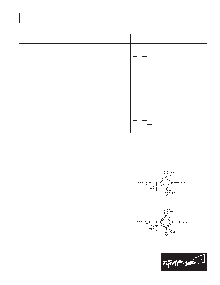
3t
6 and t17 are measured with the load circuits of Figure 1 and defined as the time required for an output to cross 0.8 V or 2.4 V.
4t
7 is derived from the measured time taken by the data outputs to change 0.5 V when loaded with the circuit of Figure 2. The measured number is then extrapolated
back to remove the effects of charging or discharging the 50 pF capacitor. This means that the time, t 7, quoted in the Timing Characteristics is the true bus relinquish
time of the part and is independent of bus loading.
5SCLK mark/space ratio (measured from a voltage level of 1.6 V) is 40/60 to 60/40.
6SDATA will drive higher capacitive loads, but this will add to t
12 since it increases the external RC time constant (4.7 k //CL) and hence the time to reach 2.4 V.
Specifications subject to change without notice.
WARNING!
ESD SENSITIVE DEVICE
CAUTION
ESD (electrostatic discharge) sensitive device. Electrostatic charges as high as 4000 V readily
accumulate on the human body and test equipment and can discharge without detection.
Although the AD7871/AD7872 features proprietary ESD protection circuitry, permanent dam-
age may occur on devices subjected to high energy electrostatic discharges. Therefore, proper
ESD precautions are recommended to avoid performance degradation or loss of functionality.
ABSOLUTE MAXIMUM RATINGS*
VDD to AGND . . . . . . . . . . . . . . . . . . . . . . . . . –0.3 V to +7 V
VSS to AGND . . . . . . . . . . . . . . . . . . . . . . . . . +0.3 V to –7 V
AGND to DGND . . . . . . . . . . . . . . . . –0.3 V to VDD + 0.3 V
VIN to AGND . . . . . . . . . . . . . . . . VSS –0.3 V to VDD + 0.3 V
REF OUT, CREF to AGND . . . . . . . . . . . . . . . . . . 0 V to VDD
Digital Inputs to DGND . . . . . . . . . . . –0.3 V to VDD + 0.3 V
Digital Outputs to DGND . . . . . . . . . . –0.3 V to VDD + 0.3 V
Operating Temperature Range
Commercial (J, K Versions) . . . . . . . . . . . . . . 0
°C to +70°C
Industrial (A, B Versions) . . . . . . . . . . . . . –40
°C to +85°C
Extended (T Version) . . . . . . . . . . . . . . . –55
°C to +125°C
Storage Temperature Range . . . . . . . . . . . . –65
°C to +150°C
Lead Temperature (Soldering, 10 sec) . . . . . . . . . . . . +300
°C
Power Dissipation (Any Package) to +75
°C . . . . . . . . 450 mW
Derates above +75
°C by . . . . . . . . . . . . . . . . . . . . . 6 mW/°C
*Stresses above those listed under “Absolute Maximum Ratings” may cause
permanent damage to the device. This is a stress rating only; functional operation
of the device at these or any other conditions above those listed in the operational
sections of this specification is not implied. Exposure to absolute maximum rating
conditions for extended periods may affect device reliability.
Figure 1. Load Circuit for Access Time
Figure 2. Load Circuit for Output Float Delay
(VDD = +5 V
5%, VSS = –5 V
5%, AGND = DGND = O V. See Figures 9, 10, 11 and 12.)
相关PDF资料 |
PDF描述 |
|---|---|
| LTC2369HMS-18#TRPBF | IC ADC 18BIT SRL/SPI 16-MSOP |
| IDT7284L12PA8 | IC FIFO 2048X18 12NS 56TSSOP |
| D38999/24FC8SD | CONN RCPT 8POS JAM NUT W/SCKT |
| MS27466T23F53PB | CONN RCPT 53POS WALL MT W/PINS |
| LTC2379HMS-18#TRPBF | IC ADC 18BIT SPI/SRL 16MSOP |
相关代理商/技术参数 |
参数描述 |
|---|---|
| AD7871KN | 功能描述:IC ADC 14BIT SAMPLING 28-DIP RoHS:否 类别:集成电路 (IC) >> 数据采集 - 模数转换器 系列:- 产品培训模块:Lead (SnPb) Finish for COTS Obsolescence Mitigation Program 标准包装:2,500 系列:- 位数:12 采样率(每秒):3M 数据接口:- 转换器数目:- 功率耗散(最大):- 电压电源:- 工作温度:- 安装类型:表面贴装 封装/外壳:SOT-23-6 供应商设备封装:SOT-23-6 包装:带卷 (TR) 输入数目和类型:- |
| AD7871KNZ | 功能描述:IC ADC 14BIT SAMPLING 28DIP RoHS:是 类别:集成电路 (IC) >> 数据采集 - 模数转换器 系列:- 标准包装:1 系列:- 位数:14 采样率(每秒):83k 数据接口:串行,并联 转换器数目:1 功率耗散(最大):95mW 电压电源:双 ± 工作温度:0°C ~ 70°C 安装类型:通孔 封装/外壳:28-DIP(0.600",15.24mm) 供应商设备封装:28-PDIP 包装:管件 输入数目和类型:1 个单端,双极 |
| AD7871KP | 功能描述:IC ADC 14BIT SAMPLING 28-PLCC RoHS:否 类别:集成电路 (IC) >> 数据采集 - 模数转换器 系列:- 产品培训模块:Lead (SnPb) Finish for COTS Obsolescence Mitigation Program 标准包装:2,500 系列:- 位数:12 采样率(每秒):3M 数据接口:- 转换器数目:- 功率耗散(最大):- 电压电源:- 工作温度:- 安装类型:表面贴装 封装/外壳:SOT-23-6 供应商设备封装:SOT-23-6 包装:带卷 (TR) 输入数目和类型:- |
| AD7871KP-REEL | 制造商:Rochester Electronics LLC 功能描述:- Tape and Reel |
| AD7871KPZ | 功能描述:IC ADC 14BIT SAMPLING 28-PLCC RoHS:是 类别:集成电路 (IC) >> 数据采集 - 模数转换器 系列:- 标准包装:1 系列:- 位数:14 采样率(每秒):83k 数据接口:串行,并联 转换器数目:1 功率耗散(最大):95mW 电压电源:双 ± 工作温度:0°C ~ 70°C 安装类型:通孔 封装/外壳:28-DIP(0.600",15.24mm) 供应商设备封装:28-PDIP 包装:管件 输入数目和类型:1 个单端,双极 |
发布紧急采购,3分钟左右您将得到回复。