- 您现在的位置:买卖IC网 > PDF目录10064 > AD7872BRZ-REEL (Analog Devices Inc)IC ADC 14BIT SAMPLING 16SOIC PDF资料下载
参数资料
| 型号: | AD7872BRZ-REEL |
| 厂商: | Analog Devices Inc |
| 文件页数: | 12/16页 |
| 文件大小: | 0K |
| 描述: | IC ADC 14BIT SAMPLING 16SOIC |
| 标准包装: | 1,000 |
| 位数: | 14 |
| 采样率(每秒): | 83k |
| 数据接口: | 串行 |
| 转换器数目: | 1 |
| 功率耗散(最大): | 95mW |
| 电压电源: | 双 ± |
| 工作温度: | -40°C ~ 85°C |
| 安装类型: | 表面贴装 |
| 封装/外壳: | 16-SOIC(0.295",7.50mm 宽) |
| 供应商设备封装: | 16-SOIC W |
| 包装: | 带卷 (TR) |
| 输入数目和类型: | 1 个单端,双极 |
AD7871/AD7872
–5–
REV. D
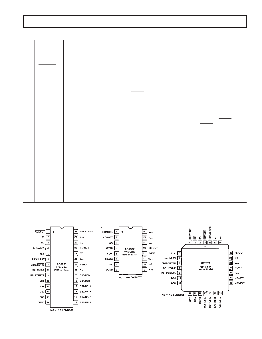
AD7872 PIN FUNCTION DESCRIPTION
DIP
No.
Mnemonic
Function
1
CONTROL
Control Input. With this pin at 0 V, the SCLK is noncontinuous; with this pin at –5 V, the SCLK
is continuous.
2
CONVST
Convert Start. A low to high transition on this input puts the track/hold into the hold mode. This
input is asynchronous to the CLK.
3
CLK
Clock Input. An external TTL-compatible clock may be applied to this input. Alternatively, tying
this pin to VSS, enables the internal laser-trimmed oscillator.
4
SSTRB
This is an active low three-state output that provides a framing pulse for serial data. An external
4.7 k
pull-up resistor is required on SSTRB.
5
SCLK
Serial Clock. SCLK is the gated serial clock output derived from the internal or external ADC
clock. If the 14/
8/CLK input is at –5 V, then the SCLK runs continuously. With CONTROL
at 0 V, it is gated off (three-state) after serial transmission is complete. SCLK is an open-drain
output and requires an external 2 k
pull-up resistor.
6
SDATA
Serial Data. This is the three-state serial data output used in conjunction with SCLK and
SSTRB in
serial data transmission. Serial data is valid on the falling edge of SCLK, when
SSTRB is low. An
external 4.7 k
pull-up resistor is required on SDATA.
7
NC
No Connect.
8
DGND
Digital Ground. Ground return for digital circuitry.
9VDD
Positive Supply for analog circuitry, +5 V
± 5%.
10
NC
No Connect.
11
CREF
Decoupling point for on-chip reference. Connect 10 nF capacitor between this pin and AGND.
12
AGND
Analog Ground. Ground reference for analog circuitry.
13
REF OUT
Voltage Reference Output. The internal 3 V reference is provided at this pin. The external load
capability is 500
A.
14
VIN
Analog Input. The input range is
±3 V.
15
VSS
Negative Supply, –5 V
± 5%.
16
VDD
Positive Supply for analog circuitry, +5 V
± 5%. Pin 16 and Pin 9 should be connected together.
PIN CONFIGURATIONS
DIP
DIP, SOIC
PLCC
相关PDF资料 |
PDF描述 |
|---|---|
| MS27467T19B32SB | CONN PLUG 32POS STRAIGHT W/SCKT |
| MS27466T21A35PA | CONN RCPT 79POS WALL MNT W/PINS |
| MS3106F28-9S | CONN PLUG 12POS STRAIGHT W/SCKT |
| MS3110F16-8S | CONN RCPT 8POS WALL MNT W/SCKT |
| MS27467T17B26SD | CONN PLUG 26POS STRAIGHT W/SCKT |
相关代理商/技术参数 |
参数描述 |
|---|---|
| AD7872JN | 制造商:Analog Devices 功能描述:ADC Single SAR 83ksps 14-bit Serial 16-Pin PDIP 制造商:Rochester Electronics LLC 功能描述:14-BIT SERIAL ADC IC - Bulk |
| AD7872JNZ | 功能描述:IC ADC 14BIT SAMPLING 16PDIP RoHS:是 类别:集成电路 (IC) >> 数据采集 - 模数转换器 系列:- 其它有关文件:TSA1204 View All Specifications 标准包装:1 系列:- 位数:12 采样率(每秒):20M 数据接口:并联 转换器数目:2 功率耗散(最大):155mW 电压电源:模拟和数字 工作温度:-40°C ~ 85°C 安装类型:表面贴装 封装/外壳:48-TQFP 供应商设备封装:48-TQFP(7x7) 包装:Digi-Reel® 输入数目和类型:4 个单端,单极;2 个差分,单极 产品目录页面:1156 (CN2011-ZH PDF) 其它名称:497-5435-6 |
| AD7872JR | 功能描述:IC ADC 14BIT LC2MOS 16-SOIC RoHS:否 类别:集成电路 (IC) >> 数据采集 - 模数转换器 系列:- 标准包装:1 系列:- 位数:14 采样率(每秒):83k 数据接口:串行,并联 转换器数目:1 功率耗散(最大):95mW 电压电源:双 ± 工作温度:0°C ~ 70°C 安装类型:通孔 封装/外壳:28-DIP(0.600",15.24mm) 供应商设备封装:28-PDIP 包装:管件 输入数目和类型:1 个单端,双极 |
| AD7872JR-REEL | 制造商:Analog Devices 功能描述: |
| AD7872JRZ | 功能描述:IC ADC 14BIT LC2MOS 16-SOIC RoHS:是 类别:集成电路 (IC) >> 数据采集 - 模数转换器 系列:- 其它有关文件:TSA1204 View All Specifications 标准包装:1 系列:- 位数:12 采样率(每秒):20M 数据接口:并联 转换器数目:2 功率耗散(最大):155mW 电压电源:模拟和数字 工作温度:-40°C ~ 85°C 安装类型:表面贴装 封装/外壳:48-TQFP 供应商设备封装:48-TQFP(7x7) 包装:Digi-Reel® 输入数目和类型:4 个单端,单极;2 个差分,单极 产品目录页面:1156 (CN2011-ZH PDF) 其它名称:497-5435-6 |
发布紧急采购,3分钟左右您将得到回复。