参数资料
| 型号: | AD7874AQ |
| 厂商: | Analog Devices Inc |
| 文件页数: | 2/16页 |
| 文件大小: | 0K |
| 描述: | IC DAS 12BIT 4CH 5V 28-CDIP |
| 标准包装: | 1 |
| 类型: | 数据采集系统(DAS) |
| 分辨率(位): | 12 b |
| 采样率(每秒): | 116k |
| 数据接口: | 并联 |
| 电压电源: | 双 ± |
| 电源电压: | ±5V |
| 工作温度: | -40°C ~ 85°C |
| 安装类型: | 通孔 |
| 封装/外壳: | 28-CDIP(0.600",15.24mm) |
| 供应商设备封装: | 28-CDIP |
| 包装: | 管件 |
AD7874
REV. C
–10–
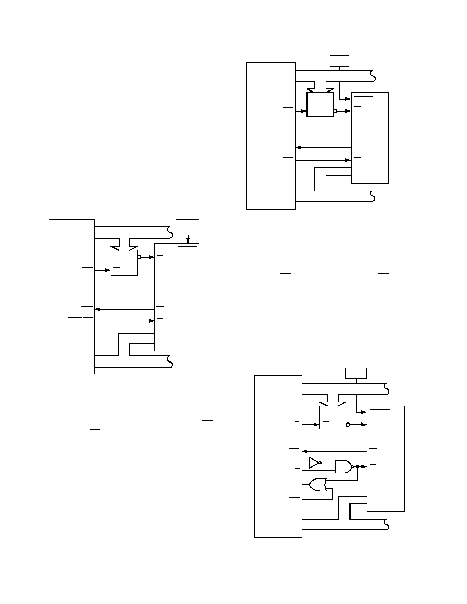
MICROPROCESSOR INTERFACING
The AD7874 high speed bus timing allows direct interfacing to
DSP processors as well as modern 16-bit microprocessors.
Suitable microprocessor interfaces are shown in Figures 12
through 16.
AD7874–ADSP-2100 Interface
Figure 12 shows an interface between the AD7874 and the
ADSP-2100. Conversion is initiated using a timer which allows
very accurate control of the sampling instant on all four chan-
nels. The AD7874 INT line provides an interrupt to the ADSP-
2100 when conversion is completed on all four channels. The
four conversion results can then be read from the AD7874 using
four successive reads to the same memory address. The follow-
ing instruction reads one of the four results (this instruction is
repeated four times to read all four results in sequence):
MR0 = DM(ADC)
where MR0 is the ADSP-2100 MR0 register and
ADC is the AD7874 address.
TIMER
DMA0
DMA13
DMD15
DMD0
DMS
EN
ADDR
DECODE
ADDRESS BUS
ADSP-2100
(ADSP-2101/
ADSP-2102)
* ADDITIONAL PINS OMITTED FOR CLARITY
DATA BUS
CONVST
CS
DB11
DB0
RD
INT
AD7874*
IRQn
DMRD (RD)
Figure 12. AD7874–ADSP-2100 Interface
AD7874–ADSP-2101/ADSP-2102 Interface
The interface outlined in Figure 12 also forms the basis for an
interface between the AD7874 and the ADSP-2101/ADSP-2102.
The READ line of the ADSP-2101/ADSP-2102 is labeled RD.
In this interface, the RD pulse width of the processor can be
programmed using the Data Memory Wait State Control Regis-
ter. The instruction used to read one of the four results is as
outlined for the ADSP-2100.
AD7874–TMS32010 Interface
An interface between the AD7874 and the TMS32010 is shown
in Figure 13. Once again the conversion is initiated using an ex-
ternal timer and the TMS32010 is interrupted when all four
conversions have been completed. The following instruction is
used to read the conversion results from the AD7874:
IN D,ADC
where D is Data Memory address and
ADC is the AD7874 address.
PA0
PA2
D15
D0
MEN
EN
ADDR
DECODE
ADDRESS BUS
TIMER
DATA BUS
CONVST
CS
DB11
DB0
RD
INT
AD7874*
TMS32010
*ADDITIONAL PINS OMITTED FOR CLARITY
INT
DEN
Figure 13. AD7874–TMS32010 Interface
AD7874–TMS320C25 Interface
Figure 14 shows an interface between the AD7874 and the
TMS320C25. As with the two previous interfaces, conversion is
initiated with a timer and the processor is interrupted when the
conversion sequence is completed. The TMS320C25 does not
have a separate RD output to drive the AD7874 RD input di-
rectly. This has to be generated from the processor STRB and
R/W outputs with the addition of some logic gates. The RD sig-
nal is OR-gated with the MSC signal to provide the one WAIT
state required in the read cycle for correct interface timing.
Conversion results are read from the AD7874 using the follow-
ing instruction:
IN D,ADC
where D is Data Memory address and
ADC is the AD7874 address.
A0
A15
D15
D0
IS
EN
ADDR
DECODE
ADDRESS BUS
TIMER
DATA BUS
CONVST
CS
DB11
DB0
RD
INT
AD7874*
TMS320C25
*ADDITIONAL PINS OMITTED FOR CLARITY
INTn
R/W
STRB
MSC
READY
Figure 14. AD7874–TMS320C25 Interface
相关PDF资料 |
PDF描述 |
|---|---|
| MAX1046BETX+T | IC ADC/DAC 10BIT 36-TQFN-EP |
| V300A5M300B2 | CONVERTER MOD DC/DC 5V 300W |
| VI-252-MY-S | CONVERTER MOD DC/DC 15V 50W |
| MAX1409CAP+T | IC DAS 16BIT LP 20-SSOP |
| V300A3V3M200BL3 | CONVERTER MOD DC/DC 3.3V 200W |
相关代理商/技术参数 |
参数描述 |
|---|---|
| AD7874AR | 功能描述:IC DAS 12BIT 4CH LC2MOS 28-SOIC RoHS:否 类别:集成电路 (IC) >> 数据采集 - ADCs/DAC - 专用型 系列:- 产品培训模块:Lead (SnPb) Finish for COTS Obsolescence Mitigation Program 标准包装:50 系列:- 类型:数据采集系统(DAS) 分辨率(位):16 b 采样率(每秒):21.94k 数据接口:MICROWIRE?,QSPI?,串行,SPI? 电压电源:模拟和数字 电源电压:1.8 V ~ 3.6 V 工作温度:-40°C ~ 85°C 安装类型:表面贴装 封装/外壳:40-WFQFN 裸露焊盘 供应商设备封装:40-TQFN-EP(6x6) 包装:托盘 |
| AD7874AR-REEL | 制造商:Analog Devices 功能描述:ADC Single SAR 116ksps 12-bit Parallel 28-Pin SOIC W T/R |
| AD7874AR-REEL7 | 功能描述:IC DAS 12BIT 4CH 5V 28-SOIC RoHS:否 类别:集成电路 (IC) >> 数据采集 - ADCs/DAC - 专用型 系列:- 产品培训模块:Lead (SnPb) Finish for COTS Obsolescence Mitigation Program 标准包装:50 系列:- 类型:数据采集系统(DAS) 分辨率(位):16 b 采样率(每秒):21.94k 数据接口:MICROWIRE?,QSPI?,串行,SPI? 电压电源:模拟和数字 电源电压:1.8 V ~ 3.6 V 工作温度:-40°C ~ 85°C 安装类型:表面贴装 封装/外壳:40-WFQFN 裸露焊盘 供应商设备封装:40-TQFN-EP(6x6) 包装:托盘 |
| AD7874ARZ | 功能描述:IC DAS 12BIT 4CH 5V 28-SOIC RoHS:是 类别:集成电路 (IC) >> 数据采集 - ADCs/DAC - 专用型 系列:- 产品培训模块:Data Converter Basics 标准包装:1 系列:- 类型:电机控制 分辨率(位):12 b 采样率(每秒):1M 数据接口:串行,并联 电压电源:单电源 电源电压:2.7 V ~ 3.6 V,4.5 V ~ 5.5 V 工作温度:-40°C ~ 85°C 安装类型:表面贴装 封装/外壳:100-TQFP 供应商设备封装:100-TQFP(14x14) 包装:剪切带 (CT) 其它名称:296-18373-1 |
| AD7874ARZ-REEL | 功能描述:IC DAS 12BIT 4CH 5V 28-SOIC RoHS:是 类别:集成电路 (IC) >> 数据采集 - ADCs/DAC - 专用型 系列:- 产品培训模块:Lead (SnPb) Finish for COTS Obsolescence Mitigation Program 标准包装:50 系列:- 类型:数据采集系统(DAS) 分辨率(位):16 b 采样率(每秒):21.94k 数据接口:MICROWIRE?,QSPI?,串行,SPI? 电压电源:模拟和数字 电源电压:1.8 V ~ 3.6 V 工作温度:-40°C ~ 85°C 安装类型:表面贴装 封装/外壳:40-WFQFN 裸露焊盘 供应商设备封装:40-TQFN-EP(6x6) 包装:托盘 |
发布紧急采购,3分钟左右您将得到回复。