参数资料
| 型号: | AD7874BQ |
| 厂商: | Analog Devices Inc |
| 文件页数: | 10/16页 |
| 文件大小: | 0K |
| 描述: | IC DAS 12BIT 4CH 5V 28-CDIP |
| 标准包装: | 1 |
| 类型: | 数据采集系统(DAS) |
| 分辨率(位): | 12 b |
| 采样率(每秒): | 116k |
| 数据接口: | 并联 |
| 电压电源: | 双 ± |
| 电源电压: | ±5V |
| 工作温度: | -40°C ~ 85°C |
| 安装类型: | 通孔 |
| 封装/外壳: | 28-CDIP(0.600",15.24mm) |
| 供应商设备封装: | 28-CDIP |
| 包装: | 管件 |
AD7874
REV. C
–3–
TIMING CHARACTERISTICS1
Parameter
A, B Versions
S Version
Units
Conditions/Comments
t1
50
ns min
CONVST
Pulse Width
t2
0
ns min
CS
to RD Setup Time
t3
60
70
ns min
RD
Pulse Width
t4
0
ns min
CS
to RD Hold Time
t5
60
ns max
RD
to INT Delay
t6
2
57
70
ns max
Data Access Time after RD
t7
3
55
ns min
Bus Relinquish Time after RD
45
50
ns max
t8
130
150
ns min
Delay Time between Reads
tCONV
31
s min
CONVST
to INT, External Clock
32.5
s max
CONVST
to INT, External Clock
31
s min
CONVST
to INT, Internal Clock
35
s max
CONVST
to INT, Internal Clock
tCLK
10
s max
Minimum Input Clock Period
NOTES
1Timing Specifications in bold print are 100% production tested. All other times are sample tested at +25
°C to ensure compliance. All input signals are specified with
tr = tf = 5 ns (10% to 90% of +5 V) and timed from a voltage level of 1.6 V.
2t
6 is measured with the load circuit of Figure 1 and defined as the time required for an output to cross 0.8 V or 2.4 V.
3t
7 is derived from the measured time taken by the data outputs to change 0.5 V when loaded with the circuit of Figure 2. The measured number is then extrapolated
back to remove the effects of charging or discharging the 50 pF capacitor. This means that the time, t 7, quoted in the timing characteristics is the true bus relinquish
time of the part and as such is independent of external bus loading capacitances.
Specifications subject to change without notice.
(VDD = +5 V
5%, VSS = –5 V
5%, AGND = DGND = O V, tCLK = 2.5 MHz external unless
otherwise noted.)
ABSOLUTE MAXIMUM RATINGS*
(TA = +25°C unless otherwise noted)
VDD to AGND . . . . . . . . . . . . . . . . . . . . . . . . . –0.3 V to +7 V
VDD to DGND . . . . . . . . . . . . . . . . . . . . . . . . . –0.3 V to +7 V
VSS to AGND . . . . . . . . . . . . . . . . . . . . . . . . . +0.3 V to –7 V
AGND to DGND . . . . . . . . . . . . . . . . –0.3 V to VDD + 0.3 V
VIN to AGND . . . . . . . . . . . . . . . . . . . . . . . . . –15 V to +15 V
REF OUT to AGND . . . . . . . . . . . . . . . . . . . . . . . 0 V to VDD
Digital Inputs to DGND . . . . . . . . . . . –0.3 V to VDD + 0.3 V
Digital Outputs to DGND . . . . . . . . . . –0.3 V to VDD + 0.3 V
Operating Temperature Range
Commercial (A, B Versions) . . . . . . . . . . . –40
°C to +85°C
Extended (S Version) . . . . . . . . . . . . . . . . –55
°C to +125°C
Storage Temperature Range . . . . . . . . . . . . –65
°C to +150°C
Lead Temperature (Soldering, 10 secs) . . . . . . . . . . . +300
°C
Power Dissipation (Any Package) to +75
°C . . . . . . 1,000 mW
Derates above +75
°C by . . . . . . . . . . . . . . . . . . . . 10 mW/°C
*Stresses above those listed under “Absolute Maximum Ratings” may cause
permanent damage to the device. This is a stress rating only and functional
operation of the device at these or any other conditions above those listed in the
operational sections of this specifications is not implied. Exposure to absolute
maximum rating conditions for extended periods may affect device reliability.
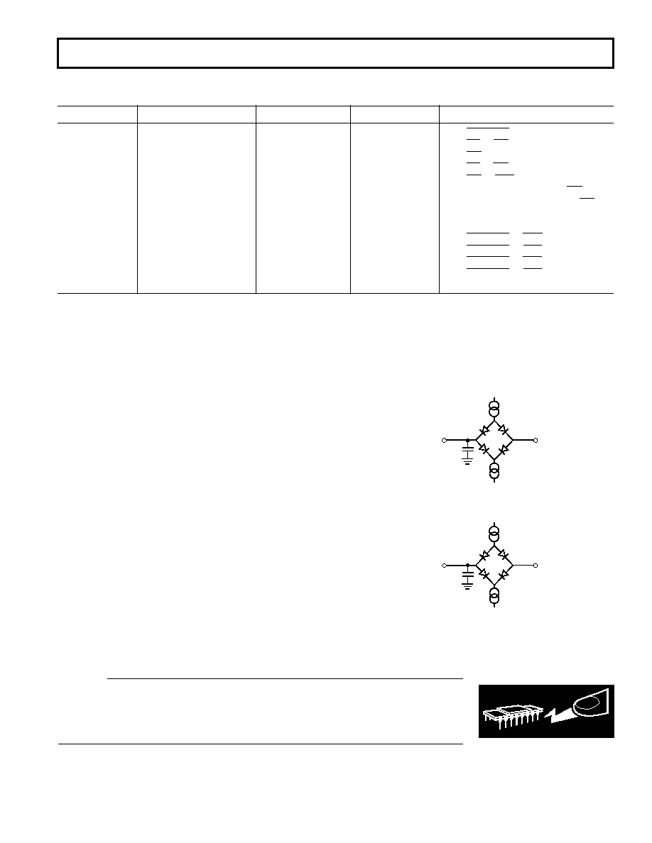
TO OUTPUT
PIN
1.6mA
2.1V
+
200
A
50pF
Figure 1. Load Circuit for Access Time
TO OUTPUT
PIN
1.6mA
2.1V
+
200
A
50pF
Figure 2. Load Circuit for Bus Relinquish Time
WARNING!
ESD SENSITIVE DEVICE
CAUTION
ESD (electrostatic discharge) sensitive device. Electrostatic charges as high as 4000 V readily
accumulate on the human body and test equipment and can discharge without detection.
Although the AD7874 features proprietary ESD protection circuitry, permanent damage may
occur on devices subjected to high energy electrostatic discharges. Therefore, proper ESD
precautions are recommended to avoid performance degradation or loss of functionality.
相关PDF资料 |
PDF描述 |
|---|---|
| AD7874AQ | IC DAS 12BIT 4CH 5V 28-CDIP |
| MAX1046BETX+T | IC ADC/DAC 10BIT 36-TQFN-EP |
| V300A5M300B2 | CONVERTER MOD DC/DC 5V 300W |
| VI-252-MY-S | CONVERTER MOD DC/DC 15V 50W |
| MAX1409CAP+T | IC DAS 16BIT LP 20-SSOP |
相关代理商/技术参数 |
参数描述 |
|---|---|
| AD7874BR | 制造商:Analog Devices 功能描述:ADC Single SAR 116ksps 12-bit Parallel 28-Pin SOIC W 制造商:Rochester Electronics LLC 功能描述:- Bulk 制造商:Analog Devices 功能描述:IC 12-BIT ADC |
| AD7874BRMZ | 制造商:Analog Devices 功能描述: |
| AD7874BRZ | 功能描述:IC DAS 12BIT 4CH LC2MOS 28-SOIC RoHS:是 类别:集成电路 (IC) >> 数据采集 - ADCs/DAC - 专用型 系列:- 产品培训模块:Lead (SnPb) Finish for COTS Obsolescence Mitigation Program 标准包装:50 系列:- 类型:数据采集系统(DAS) 分辨率(位):16 b 采样率(每秒):21.94k 数据接口:MICROWIRE?,QSPI?,串行,SPI? 电压电源:模拟和数字 电源电压:1.8 V ~ 3.6 V 工作温度:-40°C ~ 85°C 安装类型:表面贴装 封装/外壳:40-WFQFN 裸露焊盘 供应商设备封装:40-TQFN-EP(6x6) 包装:托盘 |
| AD7874SE | 功能描述:IC DAS 12BIT 4CH 5V 28-CLCC RoHS:否 类别:集成电路 (IC) >> 数据采集 - ADCs/DAC - 专用型 系列:- 产品培训模块:Lead (SnPb) Finish for COTS Obsolescence Mitigation Program 标准包装:50 系列:- 类型:数据采集系统(DAS) 分辨率(位):16 b 采样率(每秒):21.94k 数据接口:MICROWIRE?,QSPI?,串行,SPI? 电压电源:模拟和数字 电源电压:1.8 V ~ 3.6 V 工作温度:-40°C ~ 85°C 安装类型:表面贴装 封装/外壳:40-WFQFN 裸露焊盘 供应商设备封装:40-TQFN-EP(6x6) 包装:托盘 |
| AD7874SE/883B | 制造商:未知厂家 制造商全称:未知厂家 功能描述:Single-Ended Data Acquisition System |
发布紧急采购,3分钟左右您将得到回复。