- 您现在的位置:买卖IC网 > PDF目录9713 > AD7879WARUZ-RL7 (Analog Devices Inc)IC ADC 12BIT CTLR TOUCH 16TSSOP PDF资料下载
参数资料
| 型号: | AD7879WARUZ-RL7 |
| 厂商: | Analog Devices Inc |
| 文件页数: | 27/41页 |
| 文件大小: | 0K |
| 描述: | IC ADC 12BIT CTLR TOUCH 16TSSOP |
| 标准包装: | 1,000 |
| 类型: | 电阻 |
| 触摸面板接口: | 4 线 |
| 输入数/键: | 1 TSC |
| 分辨率(位): | 12 b |
| 评估套件: | * |
| 数据接口: | 串行,SPI? |
| 数据速率/采样率 (SPS,BPS): | 105k |
| 电压基准: | 内部 |
| 电源电压: | 1.6 V ~ 3.6 V |
| 工作温度: | -40°C ~ 85°C |
| 安装类型: | 表面贴装 |
| 封装/外壳: | 16-TSSOP(0.173",4.40mm 宽) |
| 供应商设备封装: | 16-TSSOP |
| 包装: | 带卷 (TR) |
第1页第2页第3页第4页第5页第6页第7页第8页第9页第10页第11页第12页第13页第14页第15页第16页第17页第18页第19页第20页第21页第22页第23页第24页第25页第26页当前第27页第28页第29页第30页第31页第32页第33页第34页第35页第36页第37页第38页第39页第40页第41页
AD7879/AD7889
Rev. C | Page 32 of 40
SERIAL INTERFACE
The AD7879 and AD7879-1 (and the AD7889 and AD7889-1)
differ only in the serial interface provided on the part. The
AD7879 and the AD7889 are available with a serial peripheral
interface (SPI). The AD7879-1 and the AD7889-1 are available
with an I2C-compatible interface. It is recommended that
addresses outside the register map not be written to.
SPI INTERFACE
The AD7879/AD7889 have a 4-wire SPI. The SPI has a data
input pin (DIN) for inputting data to the device, a data output
pin (DOUT) for reading data back from the device, and a data
clock pin (SCL) for clocking data into and out of the device. A
chip select pin (CS) enables or disables the serial interface. CS is
required for correct operation of the SPI interface. Data is
clocked out of the AD7879/AD7889 on the falling edge of SCL,
and data is clocked into the device on the rising edge of SCL.
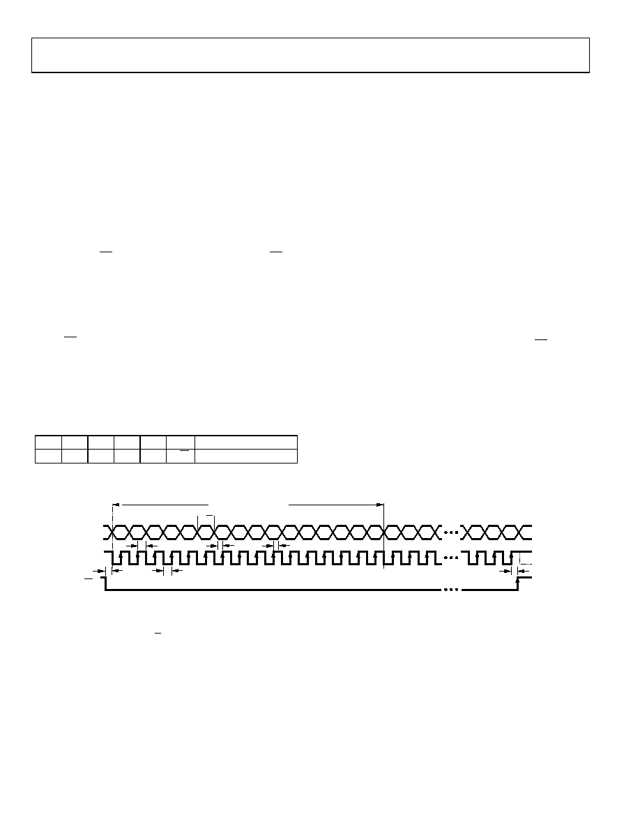
SPI Command Word
All data transactions on the SPI bus begin with the master
taking CS from high to low and sending out the command
word. This indicates to the AD7879/AD7889 whether the
transaction is a read or a write and gives the address of the
register from which to begin the data transfer. The bit map in
Table 24 shows the SPI command word.
Table 24. SPI Command Word
MSB
LSB
15
14
13
12
11
10
[9:0]
1
0
R/W
Register address
Bits[15:11] of the command word must be set to 11100 to
successfully begin a bus transaction.
Bit 10 is the read/write bit; 1 indicates a read, and 0 indicates
a write.
Bits[9:0] contain the target register address. When reading or
writing to more than one register, this address indicates the
address of the first register to be written to or read from.
Writing Data
Data is written to the AD7879/AD7889 in 16-bit words. The
first word written to the device is the command word, with the
read/write bit set to 0. The master then supplies the 16-bit input
data-word on the DIN line. The AD7879/AD7889 clock the
data into the register addressed in the command word. If there
is more than one word of data to be clocked in, the AD7879/
AD7889 automatically increment the address pointer and clock
the next data-word into the following register.
The AD7879/AD7889 continue to clock in data on the DIN line
until the master ends the write transition by pulling CS high or
until the address pointer reaches its maximum value. The AD7879/
AD7889 address pointer does not wrap. When the address
pointer reaches its maximum value, any data provided by the
master on the DIN line is ignored by the AD7879/AD7889.
NOTES
1. DATA BITS ARE LATCHED ON SCL RISING EDGES. SCL CAN IDLE HIGH OR LOW BETWEEN WRITE OPERATIONS.
2. ALL 32 BITS MUST BE WRITTEN: 16 BITS FOR THE COMMAND WORD AND 16 BITS FOR DATA.
3. 16-BIT COMMAND WORD SETTINGS FOR SINGLE WRITE OPERATION:
CW[15:11] = 11100 (ENABLE WORD)
CW[10] = 0 (R/W)
CW[9:0] = [AD9, AD8, AD7, AD6, AD5, AD4, AD3, AD2, AD1, AD0] (10-BIT MSB JUSTIFIED REGISTER ADDRESS)
CW
11
CW
10
CW
13
CW
12
DIN
CW
15
CW
14
CW
9
CW
7
CW
6
CW
5
CW
4
CW
3
CW
2
CW
1
CW
0
D2
D1
D0
CW
8
t
4
t
8
16-BIT COMMAND WORD
16-BIT DATA
5
32
6
7
8
9
10
11
12
13
14
15
16
30
31
SCL
1
2
3
4
D15
D14
D13
17
18
19
CS
ENABLE WORD
R/W
REGISTER ADDRESS
07667-
038
t
2
t
1
t
3
t
5
Figure 39. Single Register Write, SPI Timing
相关PDF资料 |
PDF描述 |
|---|---|
| AD7879-1WARUZ-RL | IC ADC 12BIT CTRLR TOUCH 16TSSOP |
| AD7879-1WACPZ-RL | IC ADC 12BIT CTRLR TOUCH 16LFCSP |
| AD7879WARUZ-RL | IC ADC 12BIT CTLR TOUCH 16TSSOP |
| AD7889-1ACBZ-RL7 | IC ADC 12BIT CTRLR TOUCH 12WLCSP |
| AD7889ACBZ-RL | IC ADC 12BIT CTRLR TOUCH 12WLCSP |
相关代理商/技术参数 |
参数描述 |
|---|---|
| AD7880BCHIPS | 功能描述:12 Bit Analog to Digital Converter 2 Input 1 SAR Die 制造商:analog devices inc. 系列:- 包装:管件 零件状态:上次购买时间 位数:12 采样率(每秒):66k 输入数:2 输入类型:单端 数据接口:并联 配置:S/H-ADC 无线电 - S/H:ADC:1:1 A/D 转换器数:1 架构:SAR 参考类型:外部,电源 电压 - 电源,模拟:5V 电压 - 电源,数字:5V 特性:- 工作温度:-40°C ~ 85°C 封装/外壳:模具 供应商器件封装:模具 标准包装:1 |
| AD7880BN | 功能描述:IC ADC 12BIT MONO LP 24-DIP RoHS:否 类别:集成电路 (IC) >> 数据采集 - 模数转换器 系列:- 标准包装:1 系列:- 位数:14 采样率(每秒):83k 数据接口:串行,并联 转换器数目:1 功率耗散(最大):95mW 电压电源:双 ± 工作温度:0°C ~ 70°C 安装类型:通孔 封装/外壳:28-DIP(0.600",15.24mm) 供应商设备封装:28-PDIP 包装:管件 输入数目和类型:1 个单端,双极 |
| AD7880BNZ | 功能描述:IC ADC 12BIT MONO LOW PWR 24DIP RoHS:是 类别:集成电路 (IC) >> 数据采集 - 模数转换器 系列:- 其它有关文件:TSA1204 View All Specifications 标准包装:1 系列:- 位数:12 采样率(每秒):20M 数据接口:并联 转换器数目:2 功率耗散(最大):155mW 电压电源:模拟和数字 工作温度:-40°C ~ 85°C 安装类型:表面贴装 封装/外壳:48-TQFP 供应商设备封装:48-TQFP(7x7) 包装:Digi-Reel® 输入数目和类型:4 个单端,单极;2 个差分,单极 产品目录页面:1156 (CN2011-ZH PDF) 其它名称:497-5435-6 |
| AD7880BQ | 制造商:Analog Devices 功能描述:ADC Single SAR 66ksps 12-bit Parallel 24-Pin CDIP 制造商:Analog Devices 功能描述:ADC SGL SAR 66KSPS 12-BIT PARALLEL 24CDIP - Rail/Tube 制造商:Rochester Electronics LLC 功能描述:- Bulk |
| AD7880BR | 功能描述:IC ADC 12BIT LC2MOS 5V LP 24SOIC RoHS:否 类别:集成电路 (IC) >> 数据采集 - 模数转换器 系列:- 标准包装:1 系列:- 位数:14 采样率(每秒):83k 数据接口:串行,并联 转换器数目:1 功率耗散(最大):95mW 电压电源:双 ± 工作温度:0°C ~ 70°C 安装类型:通孔 封装/外壳:28-DIP(0.600",15.24mm) 供应商设备封装:28-PDIP 包装:管件 输入数目和类型:1 个单端,双极 |
发布紧急采购,3分钟左右您将得到回复。