- 您现在的位置:买卖IC网 > PDF目录10160 > AD7880BRZ-REEL (Analog Devices Inc)IC ADC 12BIT MONO LP 24-SOIC PDF资料下载
参数资料
| 型号: | AD7880BRZ-REEL |
| 厂商: | Analog Devices Inc |
| 文件页数: | 3/16页 |
| 文件大小: | 0K |
| 描述: | IC ADC 12BIT MONO LP 24-SOIC |
| 标准包装: | 1,000 |
| 位数: | 12 |
| 采样率(每秒): | 66k |
| 数据接口: | 并联 |
| 转换器数目: | 1 |
| 功率耗散(最大): | 50mW |
| 电压电源: | 单电源 |
| 工作温度: | -40°C ~ 85°C |
| 安装类型: | 表面贴装 |
| 封装/外壳: | 24-SOIC(0.295",7.50mm 宽) |
| 供应商设备封装: | 24-SOIC W |
| 包装: | 带卷 (TR) |
| 输入数目和类型: | 2 个单端,单极;2 个单端,双极 |
AD7880
REV. 0
–11–
V+
+
–
C1
10F
C2
0.1F
IC1
ANALOG
INPUT
V+
V–
AB
V–
AB
LK2
LK3
TO ADC
LK1
SKT1
C3
10F
C4
0.1F
V+
V
DD
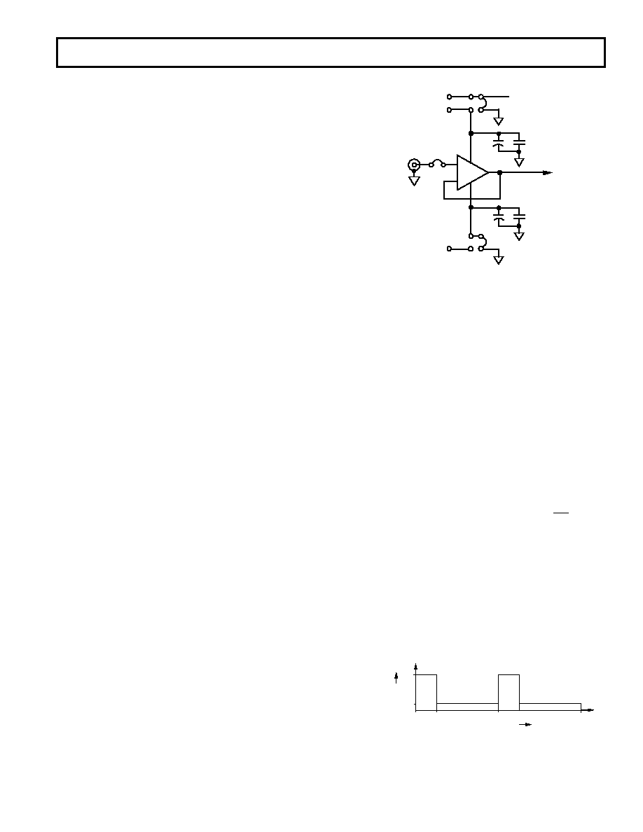
Figure 21. Analog Input Buffering
When it is required to drive the AD7880 with the 0 V to 10 V
input range, an external supply must be connected to V+ (see
Figure 21).
In bipolar operation, positive and negative supplies must be
connected to V+ and V–.
The AD711 is a general purpose op amp which could be used
to drive the analog input of the AD7880.
POWER-DOWN CONTROL (MODE INPUT)
The AD7880 is designed for systems which need to have mini-
mum power consumption. This includes such applications as
hand held, portable battery powered systems and remote moni-
toring systems. As well as consuming minimum power under
normal operating conditions, typically 20 mW, the AD7880
can be put into a power-down or sleep mode when not required
to convert signals. When in this power-down mode, the
AD7880 consumes approximately 2 mW of power.
The AD7880 is powered down by bringing the MODE input
pin to a Logic Low in conjunction with keeping the RD input
control High. The AD7880 will remain in the power-down
mode until MODE is brought to a Logic High again. The
MODE input should be driven with CD4000 or HCMOS logic
levels.
It is recommended that one “dummy” conversion be imple-
mented before reading conversion data from the AD7880 after
it has been in the power-down mode. This is required to reset
all internal logic and control circuitry. In a remote monitoring
system where, say, 10 conversions are required to be taken with
a sampling interval of 1 second, an additional 11th conversion
must be carried out. Figure 22 gives a plot of power consumption
01
2
TIME – secs
POWER
CONSUMPTION – mW
20
2
CONVERTING
POWER-DOWN
CONVERTING
POWER-DOWN
1.65 x 10
4
–
Figure 22. Power Consumption for Normal Operation
and Power-Down Operation vs. Time
APPLICATION HINTS
Good printed circuit board (PCB) layout is as important as the
circuit design itself in achieving high speed A/D performance.
The AD7880’s comparator is required to make bit decisions on
an LSB size of 1.22 mV. To achieve this, the designer must be
conscious of noise both in the ADC itself and in the preceding
analog circuitry. Switching mode power supplies are not recom-
mended, as the switching spikes will feed through to the com-
parator causing noisy code transitions. Other causes of concern
are ground loops and digital feedthrough from microprocessors.
These are factors which influence any ADC, and a proper PCB
layout which minimizes these effects is essential for best
performance.
LAYOUT HINTS
Ensure that the layout for the printed circuit board has the digi-
tal and analog signal lines separated as much as possible. Take
care not to run digital tracks alongside analog signal tracks.
Guard (screen) the analog input with AGND.
Establish a single point analog ground (star ground) separate
from the logic system ground at the AD7880 AGND pin or as
close as possible to the AD7880. Connect all other grounds and
the AD7880 DGND to this single analog ground point. Do not
connect any other digital grounds to this analog ground point.
Low impedance analog and digital power supply common re-
turns are essential to low noise operation of the ADC, so make
the foil width for these tracks as wide as possible. The use of
ground planes minimizes impedance paths and also guards the
analog circuitry from digital noise. The circuit layout of Fig-
ures 26 and 27 have both analog and digital ground planes
which are kept separated and only joined together at the
AD7880 AGND pin.
NOISE
Keep the input signal leads to VIN and signal return leads from
AGND as short as possible to minimize input noise coupling. In
applications where this is not possible, use a shielded cable be-
tween the source and the ADC. Reduce the ground circuit im-
pedance as much as possible since any potential difference in
grounds between the signal source and the ADC appears as an
error voltage in series with the input signal.
ANALOG INPUT BUFFERING
To achieve specified performance, it is recommended that the
analog input (VINA, VINB) be driven from a low impedance
source. This necessitates the use of an input buffer amplifier.
The choice of op amp will be a function of the particular appli-
cation and the desired analog input range. The data acquisition
circuit, described in this data sheet allows for various op amp
configurations. Figure 21 shows the analog input buffer circuit.
The options available to drive the supply of the op amp are:
Single +5 V (derived from PCB 5 V supply)
Dual Supply (externally supplied to V+ and V–)
±5 V, ±12 V or ±15 V
The simplest configuration is the 0 V to 5 V range of Figure 5.
A single supply 5 V op amp is recommended for such an imple-
mentation. This will allow for operation of the AD7880 in the 0
V to 5 V unipolar range without supplying an external supply to
V+ and V–. The 5 V supply is derived from the systems
+5 V VDD supply.
相关PDF资料 |
PDF描述 |
|---|---|
| ADM232LAR | IC TX/RX DUAL RS-232 5VLP 16SOIC |
| LTC2383HMS-16#TRPBF | IC ADC 16BIT 1CH 1MSPS 16-MSOP |
| SP207EET-L | IC TXRX RS232 ESD LP 24SOIC |
| ADM206ARSZ-REEL | IC TXRX RS-232 5V SD/EN 24-SSOP |
| 24291-31SG-3ES | CONN RCPT 31POS PNL MNT SKT |
相关代理商/技术参数 |
参数描述 |
|---|---|
| AD7880CN | 制造商:Analog Devices 功能描述:ADC Single SAR 66ksps 12-bit Parallel 24-Pin PDIP |
| AD7880CNZ | 功能描述:IC ADC 12BIT MONO LOW PWR 24DIP RoHS:是 类别:集成电路 (IC) >> 数据采集 - 模数转换器 系列:- 标准包装:1 系列:- 位数:14 采样率(每秒):83k 数据接口:串行,并联 转换器数目:1 功率耗散(最大):95mW 电压电源:双 ± 工作温度:0°C ~ 70°C 安装类型:通孔 封装/外壳:28-DIP(0.600",15.24mm) 供应商设备封装:28-PDIP 包装:管件 输入数目和类型:1 个单端,双极 |
| AD7880CQ | 制造商:Analog Devices 功能描述:ADC Single SAR 66ksps 12-bit Parallel 24-Pin CDIP 制造商:Rochester Electronics LLC 功能描述:12 BIT ADC IC - Bulk |
| AD7880CR | 功能描述:IC ADC 12BIT MONO LP 24-SOIC RoHS:否 类别:集成电路 (IC) >> 数据采集 - 模数转换器 系列:- 产品培训模块:Lead (SnPb) Finish for COTS Obsolescence Mitigation Program 标准包装:2,500 系列:- 位数:12 采样率(每秒):3M 数据接口:- 转换器数目:- 功率耗散(最大):- 电压电源:- 工作温度:- 安装类型:表面贴装 封装/外壳:SOT-23-6 供应商设备封装:SOT-23-6 包装:带卷 (TR) 输入数目和类型:- |
| AD7880CR-REEL | 制造商:Analog Devices 功能描述:ADC Single SAR 66ksps 12-bit Parallel 24-Pin SOIC W T/R 制造商:Analog Devices 功能描述:ADC SGL SAR 66KSPS 12-BIT PARALLEL 24SOIC W - Tape and Reel |
发布紧急采购,3分钟左右您将得到回复。