- 您现在的位置:买卖IC网 > PDF目录10041 > AD7886JP (Analog Devices Inc)IC ADC 12BIT SAMPLING HS 28-PLCC PDF资料下载
参数资料
| 型号: | AD7886JP |
| 厂商: | Analog Devices Inc |
| 文件页数: | 3/16页 |
| 文件大小: | 0K |
| 描述: | IC ADC 12BIT SAMPLING HS 28-PLCC |
| 标准包装: | 1 |
| 位数: | 12 |
| 采样率(每秒): | 1M |
| 数据接口: | 并联 |
| 转换器数目: | 1 |
| 功率耗散(最大): | 350mW |
| 电压电源: | 双 ± |
| 工作温度: | 0°C ~ 70°C |
| 安装类型: | 表面贴装 |
| 封装/外壳: | 28-LCC(J 形引线) |
| 供应商设备封装: | 28-PLCC(11.51x11.51) |
| 包装: | 管件 |
| 输入数目和类型: | 2 个单端,单极;2 个单端,双极 |
AD7886
–11–
REV. B
TIMER
DMA0
DMA13
IRQn
DMD15
DMD0
DMS
ADDRESS BUS
DATA BUS
CONVST
CS
DB11
DB0
RD
BUSY
AD7886*
ADSP-2100
*ADDITIONAL PINS OMITTED FOR CLARITY
D
Q
CLK
CLR
74HC74
DMACK
CLK
OUT
DMRD
EN
ADDR
ENCODE
5V
+
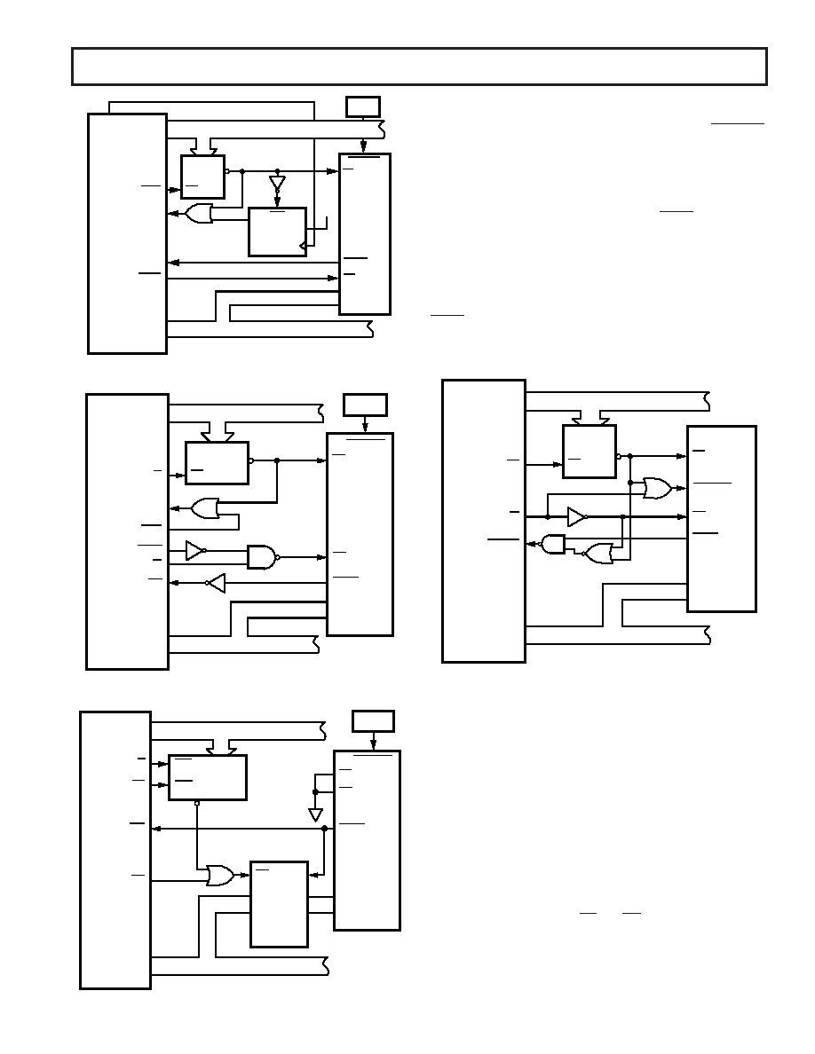
Figure 17. AD7886–ADSP-2100 Interface
ADDR
ENCODE
ADDRESS BUS
TMS320C25
CONVST
CS
AD7886*
TIMER
D15
D0
DATA BUS
DB11
DB0
INT
BUSY
RD
A0
A15
MSC
READY
IS
EN
G2
R/W
STRB
*ADDITIONAL PINS OMITTED FOR CLARITY
Figure 18. AD7886–TMS320C25 Interface
EN2
ADDR
ENCODE
ADDRESS BUS
DSP56000
D23
D0
DATA BUS
CONVST
CS
DB11
DB0
AD7886*
TIMER
IRQ
RD
A0
A15
DS
EN1
X/Y
BUSY
2X
74HC374
D11
D0
Q11
Q0
CLK
OE
*ADDITIONAL PINS OMITTED FOR CLARITY
Figure 19. AD7886–DSP56000 Interface
AD7886–MC68000
Applications requiring conversions to be initiated by the micro-
processor rather than an external timer may decode a
CONVST
signal from the address bus. An example is given in Figure 20
with the MC68000 processor. A write instruction starts conver-
sion while a read instruction reads the data when conversion is
complete. A delay at least as long as the ADC conversion time
must be allowed between initiating a conversion and reading the
ADC data into the processor. In Figure 20,
BUSY is used to
drive the processor into a WAIT state if the processor attempts
to read data before conversion is complete.
Conversion is initiated with a write instruction to the ADC:
Move.W D0,ADC
(ADC = ADC address)
Data is transferred to the processor with a read instruction;
BUSY will force the processor to WAIT for the end of conver-
sion if a conversion is in progress.
Move.W ADC,DO
(ADC = ADC address)
A0
A15
D11
D0
ADDR
ENCODE
ADDRESS BUS
DATA BUS
CONVST
CS
DB11
DB0
RD
BUSY
AD7886*
MC68000
*ADDITIONAL PINS OMITTED FOR CLARITY
R/W
EN
DTACK
AS
Figure 20. AD7886–MC68000 Interface
AD7886–Z-80/8085A
For 8-bit processors, an external latch is required to store four
bits of the conversion result (4 LSBs in Figure 21). The data is
then read in two bytes: one read from the ADC and a second
from the latch.
Figure 21 shows a typical interface suitable for the Z-80 or the
8085A. Not shown in the Figure is the 8-bit latch needed to
demultiplex the 8085A common address/data bus. The follow-
ing LOAD instruction reads the conversion result into the HL
register pair:
For the 8085A–LHLD
(ADC) (ADC = ADC address)
For the Z-80–LDHL
(ADC) (ADC = ADC address)
This is a two byte read instruction. The first byte to be read has
to be the high byte (DB11 to DB4). At the end of the first read
operation, the rising edge of
CS and RD clocks the 4 LSBs into
74HC374 latches. The second byte (4 LSBs) is then read from
these latches.
相关PDF资料 |
PDF描述 |
|---|---|
| IDT72821L10PFG8 | IC FIFO SYNC 1KX9 10NS 64QFP |
| LTC1688CS | IC DVR 100MBPS RS485 QUAD 16SOIC |
| LTC2172CUKG-14#TRPBF | IC ADC 14BIT SER/PAR 65M 52-QFN |
| D38999/26FB98PE | CONN PLUG 6POS STRAIGHT W/PINS |
| LTC1349ISW | IC TXRX 5V RS232 LOW PWR 28-SOIC |
相关代理商/技术参数 |
参数描述 |
|---|---|
| AD7886JP-REEL | 功能描述:IC ADC 12BIT SAMPLING HS 28-PLCC RoHS:否 类别:集成电路 (IC) >> 数据采集 - 模数转换器 系列:- 标准包装:1 系列:- 位数:14 采样率(每秒):83k 数据接口:串行,并联 转换器数目:1 功率耗散(最大):95mW 电压电源:双 ± 工作温度:0°C ~ 70°C 安装类型:通孔 封装/外壳:28-DIP(0.600",15.24mm) 供应商设备封装:28-PDIP 包装:管件 输入数目和类型:1 个单端,双极 |
| AD7886KP-REEL | 制造商:Analog Devices 功能描述: |
| AD7887AR | 功能描述:IC ADC 12BIT 2CH SRL 8-SOIC RoHS:否 类别:集成电路 (IC) >> 数据采集 - 模数转换器 系列:- 标准包装:1,000 系列:- 位数:16 采样率(每秒):45k 数据接口:串行 转换器数目:2 功率耗散(最大):315mW 电压电源:模拟和数字 工作温度:0°C ~ 70°C 安装类型:表面贴装 封装/外壳:28-SOIC(0.295",7.50mm 宽) 供应商设备封装:28-SOIC W 包装:带卷 (TR) 输入数目和类型:2 个单端,单极 |
| AD7887ARM | 功能描述:IC ADC 12BIT 2CH SRL 8-MSOP RoHS:否 类别:集成电路 (IC) >> 数据采集 - 模数转换器 系列:- 标准包装:1,000 系列:- 位数:16 采样率(每秒):45k 数据接口:串行 转换器数目:2 功率耗散(最大):315mW 电压电源:模拟和数字 工作温度:0°C ~ 70°C 安装类型:表面贴装 封装/外壳:28-SOIC(0.295",7.50mm 宽) 供应商设备封装:28-SOIC W 包装:带卷 (TR) 输入数目和类型:2 个单端,单极 |
| AD7887ARM-REEL | 制造商:Analog Devices 功能描述:ADC Single SAR 125ksps 12-bit Serial 8-Pin MSOP T/R |
发布紧急采购,3分钟左右您将得到回复。