- 您现在的位置:买卖IC网 > PDF目录10326 > AD7887ARMZ-REEL7 (Analog Devices Inc)IC ADC 12BIT 2CHAN SRL 8MSOP PDF资料下载
参数资料
| 型号: | AD7887ARMZ-REEL7 |
| 厂商: | Analog Devices Inc |
| 文件页数: | 3/24页 |
| 文件大小: | 0K |
| 描述: | IC ADC 12BIT 2CHAN SRL 8MSOP |
| 设计资源: | Software Calibrated, 1 MHz to 8 GHz, 70 dB RF Power Measurement System Using AD8318 (CN0150) |
| 标准包装: | 1,000 |
| 位数: | 12 |
| 采样率(每秒): | 125k |
| 数据接口: | DSP,MICROWIRE?,QSPI?,串行,SPI? |
| 转换器数目: | 1 |
| 功率耗散(最大): | 3.5mW |
| 电压电源: | 单电源 |
| 工作温度: | -40°C ~ 125°C |
| 安装类型: | 表面贴装 |
| 封装/外壳: | 8-TSSOP,8-MSOP(0.118",3.00mm 宽) |
| 供应商设备封装: | 8-MSOP |
| 包装: | 带卷 (TR) |
| 输入数目和类型: | 2 个单端,单极 |
AD7887
Rev. D | Page 11 of 24
THEORY OF OPERATION
CIRCUIT INFORMATION
The AD7887 is a fast, low power, 12-bit, single-supply, single-
channel/dual-channel ADC. The part can be operated from a
3 V (2.7 V to 3.6 V) supply or from a 5 V (4.75 V to 5.25 V) supply.
When operated from either a 5 V or 3 V supply, the AD7887 is
capable of throughput rates of 125 kSPS when provided with a
2 MHz clock.
The AD7887 provides the user with an on-chip, track/hold
analog-to-digital converter reference and a serial interface
housed in an 8-lead package. The serial clock input accesses data
from the part and provides the clock source for the successive
approximation ADC. The part can be configured for single-
channel or dual-channel operation. When configured as a
single-channel part, the analog input range is 0 to VREF (where the
externally applied VREF can be between 1.2 V and VDD). When
the AD7887 is configured for two input channels, the input
range is determined by internal connections to be 0 to VDD.
If single-channel operation is required, the AD7887 can be
operated in a read-only mode by tying the DIN line permanently
to GND. For applications where the user wants to change the
mode of operation or wants to operate the AD7887 as a dual-
channel ADC, the DIN line can be used to clock data into the
part’s control register.
CONVERTER OPERATION
The AD7887 is a successive approximation ADC built around a
schematics of the ADC. Figure 8 shows the ADC during its
acquisition phase. SW2 is closed and SW1 is in Position A, the
comparator is held in a balanced condition, and the sampling
capacitor acquires the signal on AIN.
(REF IN/REF OUT)/2
SAMPLING
CAPACITOR
COMPARATOR
ACQUISITION
PHASE
SW1
A
SW2
AGND
B
AIN
CHARGE
REDISTRIBUTION
DAC
CONTROL
LOGIC
06
19
1-
0
08
Figure 8. ADC Acquisition Phase
When the ADC starts a conversion (see Figure 9), SW2 opens
and SW1 moves to Position B, causing the comparator to become
unbalanced. The control logic and the charge-redistribution DAC
are used to add and subtract fixed amounts of charge from the
sampling capacitor to bring the comparator back into a balanced
condition. When the comparator is rebalanced, the conversion
is complete. The control logic generates the ADC output code.
Figure 10 shows the ADC transfer function.
(REF IN/REF OUT)/2
SAMPLING
CAPACITOR
COMPARATOR
CONVERSION
PHASE
SW1
A
SW2
AGND
B
VIN
CHARGE
REDISTRIBUTION
DAC
CONTROL
LOGIC
06
19
1-
00
9
Figure 9. ADC Conversion Phase
ADC TRANSFER FUNCTION
The output coding of the AD7887 is straight binary. The
designed code transitions occur at successive integer LSB values
(that is, 1 LSB, 2 LSB, and so on). The LSB size is VREF/4096. The
ideal transfer characteristic for the AD7887 is shown in Figure
0V
ADC
CO
DE
ANALOG INPUT
111 ... 000
011 ... 111
0.5LSB
+VREF – 1.5LSB
1LSB = VREF/4096
111 ... 111
111 ... 110
000 ... 010
000 ... 001
000 ... 000
06
19
1
-01
0
Figure 10. Transfer Characteristic
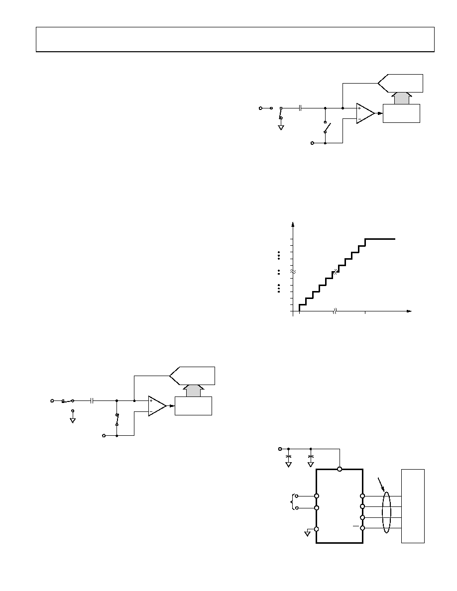
TYPICAL CONNECTION DIAGRAM
Figure 11 shows a typical connection diagram for the AD7887.
The GND pin is connected to the analog ground plane of the
system. The part is in dual-channel mode so VREF is internally
connected to a well-decoupled VDD pin to provide an analog
input range of 0 V to VDD. The conversion result is output in a
16-bit word with four leading zeros followed by the MSB of the
12-bit result. For applications where power consumption is of
concern, the automatic power-down at the end of conversion
should be used to improve power performance. See the Modes
of Operation section.
DOUT
DIN
SCLK
CS
AIN1
AIN2
GND
0.1F
10F
SUPPLY 2.7V
TO 5.25V
SERIAL
INTERFACE
VDD
AD7887
0V TO VDD
INPUT
C/P
06
19
1-
01
1
Figure 11. Typical Connection Diagram
相关PDF资料 |
PDF描述 |
|---|---|
| AD7813YRZ-REEL7 | IC ADC 10BIT PARALLEL 16SOIC |
| VI-BWF-MW-S | CONVERTER MOD DC/DC 72V 100W |
| AD7813YRUZ-REEL7 | IC ADC 10BIT PARALLEL 16TSSOP |
| VI-BWD-MW-S | CONVERTER MOD DC/DC 85V 100W |
| D38999/20ME8SNLC | CONN HSG RCPT 8POS WALL MT SCKT |
相关代理商/技术参数 |
参数描述 |
|---|---|
| AD7887AR-REEL | 制造商:Analog Devices 功能描述:ADC Single SAR 125ksps 12-bit Serial 8-Pin SOIC N T/R |
| AD7887AR-REEL7 | 功能描述:IC ADC 12BIT 2CH SRL 8-SOIC RoHS:否 类别:集成电路 (IC) >> 数据采集 - 模数转换器 系列:- 标准包装:1,000 系列:- 位数:16 采样率(每秒):45k 数据接口:串行 转换器数目:2 功率耗散(最大):315mW 电压电源:模拟和数字 工作温度:0°C ~ 70°C 安装类型:表面贴装 封装/外壳:28-SOIC(0.295",7.50mm 宽) 供应商设备封装:28-SOIC W 包装:带卷 (TR) 输入数目和类型:2 个单端,单极 |
| AD7887ARZ | 功能描述:IC ADC 12BIT SRL 125KSPS 8SOIC RoHS:是 类别:集成电路 (IC) >> 数据采集 - 模数转换器 系列:- 其它有关文件:TSA1204 View All Specifications 标准包装:1 系列:- 位数:12 采样率(每秒):20M 数据接口:并联 转换器数目:2 功率耗散(最大):155mW 电压电源:模拟和数字 工作温度:-40°C ~ 85°C 安装类型:表面贴装 封装/外壳:48-TQFP 供应商设备封装:48-TQFP(7x7) 包装:Digi-Reel® 输入数目和类型:4 个单端,单极;2 个差分,单极 产品目录页面:1156 (CN2011-ZH PDF) 其它名称:497-5435-6 |
| AD7887ARZ | 制造商:Analog Devices 功能描述:IC 12-BIT ADC |
| AD7887ARZ-REEL | 功能描述:IC ADC 12BIT 2CHAN SRL 8SOIC RoHS:是 类别:集成电路 (IC) >> 数据采集 - 模数转换器 系列:- 产品培训模块:Lead (SnPb) Finish for COTS Obsolescence Mitigation Program 标准包装:2,500 系列:- 位数:12 采样率(每秒):3M 数据接口:- 转换器数目:- 功率耗散(最大):- 电压电源:- 工作温度:- 安装类型:表面贴装 封装/外壳:SOT-23-6 供应商设备封装:SOT-23-6 包装:带卷 (TR) 输入数目和类型:- |
发布紧急采购,3分钟左右您将得到回复。