- 您现在的位置:买卖IC网 > PDF目录10325 > AD7887ARZ-REEL7 (Analog Devices Inc)IC ADC 12BIT 2CHAN SRL 8SOIC PDF资料下载
参数资料
| 型号: | AD7887ARZ-REEL7 |
| 厂商: | Analog Devices Inc |
| 文件页数: | 9/24页 |
| 文件大小: | 0K |
| 描述: | IC ADC 12BIT 2CHAN SRL 8SOIC |
| 设计资源: | Software Calibrated, 1 MHz to 8 GHz, 70 dB RF Power Measurement System Using AD8318 (CN0150) |
| 标准包装: | 1,000 |
| 位数: | 12 |
| 采样率(每秒): | 125k |
| 数据接口: | DSP,MICROWIRE?,QSPI?,串行,SPI? |
| 转换器数目: | 1 |
| 功率耗散(最大): | 3.5mW |
| 电压电源: | 单电源 |
| 工作温度: | -40°C ~ 125°C |
| 安装类型: | 表面贴装 |
| 封装/外壳: | 8-SOIC(0.154",3.90mm 宽) |
| 供应商设备封装: | 8-SO |
| 包装: | 带卷 (TR) |
| 输入数目和类型: | 2 个单端,单极 |
AD7887
Rev. D | Page 17 of 24
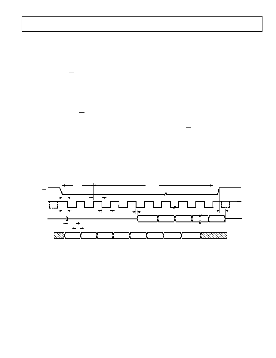
SERIAL INTERFACE
Figure 21 shows the detailed timing diagrams for serial
interfacing to the AD7887. The serial clock provides the
conversion clock and also controls the transfer of information
to and from the AD7887 during conversion.
CS initiates the data transfer and conversion process. For some
modes, the falling edge of CS wakes up the part. In all cases, it
gates the serial clock to the AD7887 and puts the on-chip
track/hold into track mode. The input signal is sampled on the
second rising edge of the SCLK input after the falling edge of
CS. Thus, the first one and one-half clock cycles after the falling
edge of CS are when the acquisition of the input signal takes
place. This time is denoted as the acquisition time (tACQ). In
modes where the falling edge of CS wakes up the part, the
acquisition time must allow for the wake-up time of 5 μs. The
on-chip track/hold goes from track mode to hold mode on the
second rising edge of SCLK, and a conversion is also initiated
on this edge. The conversion process takes an additional
fourteen and one-half SCLK cycles to complete. The rising edge
of CS puts the bus back into three-state. If CS is left low, a new
conversion can be initiated.
In dual-channel operation, the input channel that is sampled is
the one that was selected in the previous write to the control
register. Thus, in dual-channel operation, the user must write
the channel address for the next conversion while the present
conversion is in progress.
Writing of information to the control register takes place on the
first eight rising edges of SCLK in a data transfer. The control
register is always written to when a data transfer takes place.
However, the AD7887 can be operated in a read-only mode by
tying DIN low, thereby loading all 0s to the control register
every time. When operating the AD7887 in write/read mode,
the user must be careful to always set up the correct
information on the DIN line when reading data from the part.
Sixteen serial clock cycles are required to perform the con-
version process and to access data from the AD7887. In
applications where the first serial clock edge following CS going
low is a falling edge, this edge clocks out the first leading zero.
Thus, the first rising clock edge on the SCLK clock has the first
leading zero provided. In applications where the first serial
clock edge following CS going low is a rising edge, the first
leading zero may not be set up in time for the processor to read
it correctly. However, subsequent bits are clocked out on the
falling edge of SCLK so that they are provided to the processor
on the following rising edge. Thus, the second leading zero is
clocked out on the falling edge subsequent to the first rising
edge. The final bit in the data transfer is valid on the 16th rising
edge, having been clocked out on the previous falling edge.
DONTC
ZERO
0
M
P
1
M
P
H
C
L
A
U
D
/
N
I
S
F
E
R
SCLK
6
5
1
15
DOUT
DIN
23
4
16
t1
tACQ
tCONVERT
t2
t6
t7
t3
t8
DB11
DB0
DB10
DB9
THREE-
STATE
FOUR LEADING ZEROS
CS
THREE-
STATE
t4
t5
06
19
1-
0
21
Figure 21. Serial Interface Timing Diagram
相关PDF资料 |
PDF描述 |
|---|---|
| LTC2498CUHF#TRPBF | IC ADC 24BIT 16CH 38-QFN |
| D38999/26WJ61PNLC | CONN HSG PLUG 61POS STRGHT PINS |
| LTC2430IGN#TRPBF | IC ADC 20BIT DIFFINPUT/REF16SSOP |
| LTC2435-1IGN#TRPBF | IC ADC DIFF I/REF 20BIT 16-SSOP |
| LTC2435-1IGN#TR | IC CONV A/D 20BIT DIFF 16-SSOP |
相关代理商/技术参数 |
参数描述 |
|---|---|
| AD7887BR | 功能描述:IC ADC 12BIT 2CH SRL 8-SOIC RoHS:否 类别:集成电路 (IC) >> 数据采集 - 模数转换器 系列:- 标准包装:1,000 系列:- 位数:16 采样率(每秒):45k 数据接口:串行 转换器数目:2 功率耗散(最大):315mW 电压电源:模拟和数字 工作温度:0°C ~ 70°C 安装类型:表面贴装 封装/外壳:28-SOIC(0.295",7.50mm 宽) 供应商设备封装:28-SOIC W 包装:带卷 (TR) 输入数目和类型:2 个单端,单极 |
| AD7887BR-REEL | 功能描述:IC ADC 12BIT 2CH SRL 8-SOIC RoHS:否 类别:集成电路 (IC) >> 数据采集 - 模数转换器 系列:- 标准包装:1,000 系列:- 位数:16 采样率(每秒):45k 数据接口:串行 转换器数目:2 功率耗散(最大):315mW 电压电源:模拟和数字 工作温度:0°C ~ 70°C 安装类型:表面贴装 封装/外壳:28-SOIC(0.295",7.50mm 宽) 供应商设备封装:28-SOIC W 包装:带卷 (TR) 输入数目和类型:2 个单端,单极 |
| AD7887BR-REEL7 | 功能描述:IC ADC 12BIT 2CH SRL 8-SOIC RoHS:否 类别:集成电路 (IC) >> 数据采集 - 模数转换器 系列:- 标准包装:1,000 系列:- 位数:16 采样率(每秒):45k 数据接口:串行 转换器数目:2 功率耗散(最大):315mW 电压电源:模拟和数字 工作温度:0°C ~ 70°C 安装类型:表面贴装 封装/外壳:28-SOIC(0.295",7.50mm 宽) 供应商设备封装:28-SOIC W 包装:带卷 (TR) 输入数目和类型:2 个单端,单极 |
| AD7887BRZ | 功能描述:IC ADC 12BIT 2CHAN SRL 8SOIC RoHS:是 类别:集成电路 (IC) >> 数据采集 - 模数转换器 系列:- 其它有关文件:TSA1204 View All Specifications 标准包装:1 系列:- 位数:12 采样率(每秒):20M 数据接口:并联 转换器数目:2 功率耗散(最大):155mW 电压电源:模拟和数字 工作温度:-40°C ~ 85°C 安装类型:表面贴装 封装/外壳:48-TQFP 供应商设备封装:48-TQFP(7x7) 包装:Digi-Reel® 输入数目和类型:4 个单端,单极;2 个差分,单极 产品目录页面:1156 (CN2011-ZH PDF) 其它名称:497-5435-6 |
| AD7887BRZ-REEL | 功能描述:IC ADC 12BIT 2CHAN SRL 8SOIC RoHS:是 类别:集成电路 (IC) >> 数据采集 - 模数转换器 系列:- 标准包装:1,000 系列:- 位数:16 采样率(每秒):45k 数据接口:串行 转换器数目:2 功率耗散(最大):315mW 电压电源:模拟和数字 工作温度:0°C ~ 70°C 安装类型:表面贴装 封装/外壳:28-SOIC(0.295",7.50mm 宽) 供应商设备封装:28-SOIC W 包装:带卷 (TR) 输入数目和类型:2 个单端,单极 |
发布紧急采购,3分钟左右您将得到回复。