- 您现在的位置:买卖IC网 > PDF目录9712 > AD7889ACBZ-500R7 (Analog Devices Inc)IC ADC 12BIT CTRLR TOUCH 12WLCSP PDF资料下载
参数资料
| 型号: | AD7889ACBZ-500R7 |
| 厂商: | Analog Devices Inc |
| 文件页数: | 17/41页 |
| 文件大小: | 0K |
| 描述: | IC ADC 12BIT CTRLR TOUCH 12WLCSP |
| 产品变化通告: | 8mm Carrier Tape Changes 28/Feb/2012 |
| 标准包装: | 1 |
| 类型: | 电阻 |
| 触摸面板接口: | 4 线 |
| 输入数/键: | 1 TSC |
| 分辨率(位): | 12 b |
| 数据接口: | 串行,SPI? |
| 数据速率/采样率 (SPS,BPS): | 105k |
| 电压基准: | 外部 |
| 电源电压: | 1.6 V ~ 3.6 V |
| 电流 - 电源: | 10nA |
| 工作温度: | -40°C ~ 85°C |
| 安装类型: | 表面贴装 |
| 封装/外壳: | 12-UFBGA,WLCSP |
| 供应商设备封装: | 12-WLCSP |
| 包装: | 标准包装 |
| 其它名称: | AD7889ACBZ-500R7DKR |
第1页第2页第3页第4页第5页第6页第7页第8页第9页第10页第11页第12页第13页第14页第15页第16页当前第17页第18页第19页第20页第21页第22页第23页第24页第25页第26页第27页第28页第29页第30页第31页第32页第33页第34页第35页第36页第37页第38页第39页第40页第41页
AD7879/AD7889
Rev. C | Page 23 of 40
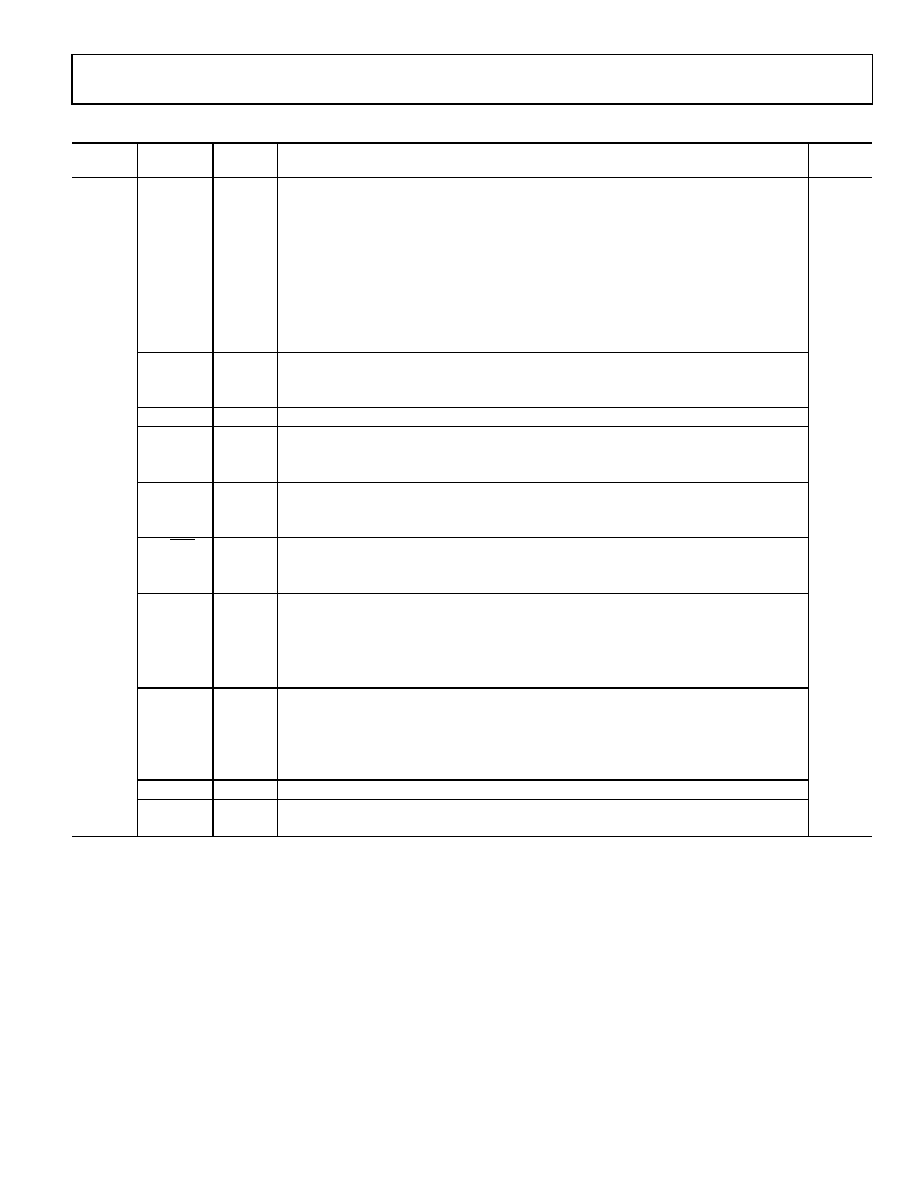
Table 13. Control Register 2
Address
Bit Name
Data Bit
Description
Default
Value
0x02
PM[1:0]
[15:14]
ADC power management.
0x4040
00 = full shutdown; the ADC, oscillator, bias, and temperature sensor are all powered down.
01 = analog blocks to be powered down depend on the ADC mode.
If ADC mode is master mode, the ADC, oscillator, bias, and temperature sensor are powered
down and must wake up when the user touches the screen.
If ADC mode is slave mode, the ADC and temperature sensor are powered down when not
being used. They wake up automatically when required. The oscillator and bias are powered
up because they are needed to measure time. This also applies to the single-conversion mode.
10 = ADC, bias, and oscillator are powered up continuously, irrespective of ADC mode.
11 = same as 01.
GPIO EN
13
GPIO enable.
0 = AUX/VBAT channel active.
1 = GPIO enabled on AUX/VBAT/GPIO pin.
GPIO DAT
12
GPIO data bit.
GPIO DIR
11
GPIO direction.
0 = output.
1 = input.
GPIO POL
10
GPIO polarity.
0 = GPIO pin is active low.
1 = GPIO pin is active high.
SER/DFR
9
Selects normal (single-ended) or ratiometric (differential) conversion.
0 = ratiometric (differential).
1 = normal (single-ended).
AVG[1:0]
[8:7]
ADC averaging.
00 = 2 middle values averaged (one measurement when median filter is disabled).
01 = 4 middle values averaged.
10 = 8 middle values averaged.
11 = 16 values averaged.
MED[1:0]
[6:5]
Median filter size.
00 = median filter disabled.
01 = 4 measurements.
10 = 8 measurements.
11 = 16 measurements.
SW/RST
4
Software reset; digital logic is reset when this bit is set.
FCD[3:0]
[3:0]
ADC first conversion delay.1
Starts at 128 s (default) and continues to 4.096 ms in steps of 128 s (see Table 22).
1
This delay occurs before conversion of the X and Y coordinate channels (including Z1 and Z2) to allow for screen settling and before the first conversion to allow the
ADC to power up.
相关PDF资料 |
PDF描述 |
|---|---|
| SSTUB32S868DHLF | IC REGIST BUFF 25BIT DDR2 176BGA |
| MS3106F24-6S | CONN PLUG 8POS STRAIGHT W/SCKT |
| D38999/24FJ61SB | CONN RCPT 61POS JAM NUT W/SCKT |
| MS27499E24A35SB | CONN RCPT 128POS BOX MNT W/SCKT |
| MS27473E18B66SD | CONN PLUG 66POS STRAIGHT W/SCKT |
相关代理商/技术参数 |
参数描述 |
|---|---|
| AD7889ACBZ-RL | 功能描述:IC ADC 12BIT CTRLR TOUCH 12WLCSP RoHS:是 类别:集成电路 (IC) >> 数据采集 - 触摸屏控制器 系列:- 标准包装:96 系列:- 类型:- 触摸面板接口:- 输入数/键:- 分辨率(位):- 评估套件:* 数据接口:- 数据速率/采样率 (SPS,BPS):- 电压基准:- 电源电压:- 电流 - 电源:- 工作温度:- 安装类型:表面贴装 封装/外壳:16-TSSOP(0.173",4.40mm 宽) 供应商设备封装:16-TSSOP 包装:带卷 (TR) |
| AD7890ACHIPS-2 | 功能描述:Data Acquisition System (DAS) 12 bit 117k SPI Die 制造商:analog devices inc. 系列:- 包装:管件 零件状态:上次购买时间 类型:数据采集系统(DAS) 分辨率(位):12 b 采样率(每秒):117k 数据接口:SPI 电压源:单电源 电压 - 电源:5V 工作温度:-40°C ~ 85°C 安装类型:表面贴装 封装/外壳:模具 供应商器件封装:模具 标准包装:1 |
| AD7890AN-10 | 功能描述:IC DAS 12BIT 8CH 24-DIP RoHS:否 类别:集成电路 (IC) >> 数据采集 - ADCs/DAC - 专用型 系列:- 产品培训模块:Lead (SnPb) Finish for COTS Obsolescence Mitigation Program 标准包装:50 系列:- 类型:数据采集系统(DAS) 分辨率(位):16 b 采样率(每秒):21.94k 数据接口:MICROWIRE?,QSPI?,串行,SPI? 电压电源:模拟和数字 电源电压:1.8 V ~ 3.6 V 工作温度:-40°C ~ 85°C 安装类型:表面贴装 封装/外壳:40-WFQFN 裸露焊盘 供应商设备封装:40-TQFN-EP(6x6) 包装:托盘 |
| AD7890AN-2 | 功能描述:IC DAS 12BIT 8CH 24-DIP RoHS:否 类别:集成电路 (IC) >> 数据采集 - ADCs/DAC - 专用型 系列:- 产品培训模块:Lead (SnPb) Finish for COTS Obsolescence Mitigation Program 标准包装:50 系列:- 类型:数据采集系统(DAS) 分辨率(位):16 b 采样率(每秒):21.94k 数据接口:MICROWIRE?,QSPI?,串行,SPI? 电压电源:模拟和数字 电源电压:1.8 V ~ 3.6 V 工作温度:-40°C ~ 85°C 安装类型:表面贴装 封装/外壳:40-WFQFN 裸露焊盘 供应商设备封装:40-TQFN-EP(6x6) 包装:托盘 |
| AD7890AN-4 | 制造商:Analog Devices 功能描述:ADC Single SAR 117ksps 12-bit Serial 24-Pin PDIP 制造商:Rochester Electronics LLC 功能描述:8 CHANNEL,SERIAL A/D IC - Bulk |
发布紧急采购,3分钟左右您将得到回复。