参数资料
| 型号: | AD7890ANZ-10 |
| 厂商: | Analog Devices Inc |
| 文件页数: | 14/28页 |
| 文件大小: | 0K |
| 描述: | IC DAS 12BIT 8CH 24-DIP |
| 标准包装: | 15 |
| 类型: | 数据采集系统(DAS) |
| 分辨率(位): | 12 b |
| 采样率(每秒): | 117k |
| 数据接口: | 串行 |
| 电压电源: | 单电源 |
| 电源电压: | 5V |
| 工作温度: | -40°C ~ 85°C |
| 安装类型: | 通孔 |
| 封装/外壳: | 24-DIP(0.300",7.62mm) |
| 供应商设备封装: | 24-PDIP |
| 包装: | 管件 |
第1页第2页第3页第4页第5页第6页第7页第8页第9页第10页第11页第12页第13页当前第14页第15页第16页第17页第18页第19页第20页第21页第22页第23页第24页第25页第26页第27页第28页
AD7890
Rev. C | Page 21 of 28
The serial clock rate from the 68HC11 is limited to significantly
less than the allowable input serial clock frequency with which
the AD7890 can operate. As a result, the time to read data from
the part is actually longer than the conversion time of the part.
This means that the AD7890 cannot run at its maximum
throughput rate when used with the 68HC11.
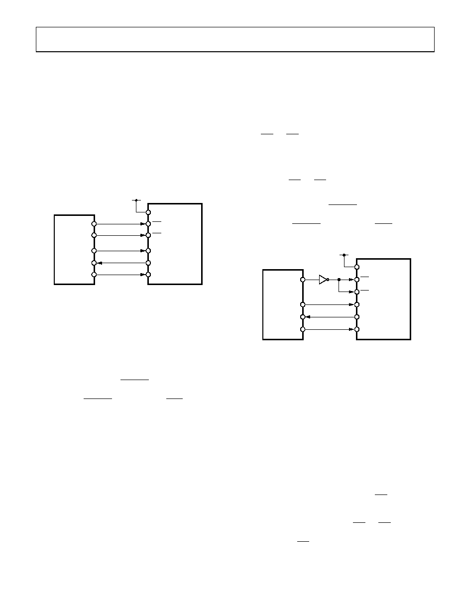
AD7890 TO ADSP-2101 INTERFACE
An interface circuit between the AD7890 and the ADSP-2101
DSP processor is shown in Figure 16. The AD7890 is
configured for its external clocking mode with the ADSP-2101
providing the serial clock and frame synchronization signals.
The RFS1 and TFS1 inputs and outputs are configured for
active low operation.
DVDD
SMODE
RFS
TFS
DATA OUT
DATA IN
SCLK
RFS1
TFS1
SCLK1
DR1
DT1
AD7890
ADSP-2101
01
35
7-
01
6
Figure 16. AD7890 to ADSP-2101 Interface
In the scheme shown, the maximum serial clock frequency the
ADSP-2101 can provide is 6.25 MHz. This allows the AD7890
to be operated at a sample rate of 111 kHz. If it is desirable to
operate the AD7890 at its maximum throughput rate of
117 kHz, an external serial clock of 10 MHz can be provided
to drive the serial clock input of both the AD7890 and the
ADSP-2101.
To monitor the conversion time on the AD7890, a scheme, such
as the scheme outlined with CONVST in the Simplifying the
Interface section, can be used. This can be implemented by
connecting the CONVST line directly to the IRQ2 input of the
ADSP-2101. An alternative to this, where the user does not have
to worry about monitoring the conversion status, is to operate
the AD7890 in its self-clocking mode. In this scheme, the actual
interface connections would remain the same as in Figure 16,
but now the AD7890 provides the serial clock and receive frame
synchronization signals. Using the AD7890 in its self-clocking
mode limits the throughput rate of the system as the serial clock
rate is limited to 2.5 MHz.
AD7890 TO DSP56000 INTERFACE
Figure 17 shows an interface circuit between the AD7890 and
the DSP56000 DSP processor. The AD7890 is configured for its
external clocking mode. The DSP56000 is configured for
normal mode, synchronous operation with continuous clock. It
is also set up for a 16-bit word with SCK and SC2 as outputs.
The FSL bit of the DSP56000 should be set to 0.
The RFS and TFS inputs of the AD7890 are connected together
so data is transmitted to and from the AD7890 at the same time.
With the DSP56000 in synchronous mode, it provides a
common frame synchronization pulse for read and write
operations on its SC2 output. This is inverted before being
applied to the RFS and TFS inputs of the AD7890.
To monitor the conversion time on the AD7890, a scheme, such
as the scheme outlined with CONVST in the Simplifying the
Interface section, can be used. This can be implemented by
connecting the CONVST line directly to the IRQA input of the
DSP56000.
DVDD
SMODE
RFS
TFS
DATA OUT
DATA IN
SCLK
SC2
SCK
SRD
STD
AD7890
DSP56000
0
135
7-
0
17
Figure 17. AD7890 to DSP56000 Interface
AD7890 TO TMS320C25/30 INTERFACE
Figure 18 shows an interface circuit between the AD7890 and
the TMS320C25/30 DSP processor. The AD7890 is configured
for its self-clocking mode where it provides the serial clock and
frame synchronization signals. However, the TMS320C25/30
requires a continuous serial clock. In the scheme outlined here,
the AD7890’s master clock signal, CLK IN, is used to provide
the serial clock for the processor. The AD7890 output SCLK, to
which the serial data is referenced, is a delayed version of the
CLK IN signal. The typical delay between the CLK IN and
SCLK is 20 ns and is no more than 50 ns over supplies and
temperature. Therefore, there is still sufficient setup time for
DATA OUT to be clocked into the DSP on the edges of the
CLK IN signal. When writing data to the AD7890, the
processor’s data hold time is sufficiently long to cater for the
delay between the two clocks. The AD7890’s RFS signal
connects to both the FSX and FSR inputs of the processor. The
processor can generate its own FSX signal, so if required, the
interface can be modified so that the RFS and TFS signals are
separated and the processor generates the FSX signal which is
connected to the TFS input of the AD7890.
相关PDF资料 |
PDF描述 |
|---|---|
| LTC1292BCN8#PBF | IC DATA ACQ SYSTEM 12BIT 8-DIP |
| MS27656E19F35SA | CONN RCPT 66POS WALL MNT W/SCKT |
| LTC1292BCN8 | IC DATA ACQ SYSTEM 12BIT 8-DIP |
| LTC1291BCN8#PBF | IC DATA ACQ SYSTEM 12BIT 8-DIP |
| M83723/75W1404Y | CONN PLUG 4POS STRAIGHT W/SCKT |
相关代理商/技术参数 |
参数描述 |
|---|---|
| AD7890ANZ-10 | 制造商:Analog Devices 功能描述:A/D Converter (A-D) IC |
| AD7890ANZ-2 | 功能描述:IC DAS 12BIT 8CH 24-DIP RoHS:是 类别:集成电路 (IC) >> 数据采集 - ADCs/DAC - 专用型 系列:- 产品培训模块:Lead (SnPb) Finish for COTS Obsolescence Mitigation Program 标准包装:50 系列:- 类型:数据采集系统(DAS) 分辨率(位):16 b 采样率(每秒):21.94k 数据接口:MICROWIRE?,QSPI?,串行,SPI? 电压电源:模拟和数字 电源电压:1.8 V ~ 3.6 V 工作温度:-40°C ~ 85°C 安装类型:表面贴装 封装/外壳:40-WFQFN 裸露焊盘 供应商设备封装:40-TQFN-EP(6x6) 包装:托盘 |
| AD7890ANZ-4 | 功能描述:IC DAS 12BIT 8CH 24-DIP RoHS:是 类别:集成电路 (IC) >> 数据采集 - ADCs/DAC - 专用型 系列:- 产品培训模块:Lead (SnPb) Finish for COTS Obsolescence Mitigation Program 标准包装:50 系列:- 类型:数据采集系统(DAS) 分辨率(位):16 b 采样率(每秒):21.94k 数据接口:MICROWIRE?,QSPI?,串行,SPI? 电压电源:模拟和数字 电源电压:1.8 V ~ 3.6 V 工作温度:-40°C ~ 85°C 安装类型:表面贴装 封装/外壳:40-WFQFN 裸露焊盘 供应商设备封装:40-TQFN-EP(6x6) 包装:托盘 |
| AD7890AR-10 | 功能描述:IC DAS 12BIT 8CH 24-SOIC RoHS:否 类别:集成电路 (IC) >> 数据采集 - ADCs/DAC - 专用型 系列:- 产品培训模块:Lead (SnPb) Finish for COTS Obsolescence Mitigation Program 标准包装:50 系列:- 类型:数据采集系统(DAS) 分辨率(位):16 b 采样率(每秒):21.94k 数据接口:MICROWIRE?,QSPI?,串行,SPI? 电压电源:模拟和数字 电源电压:1.8 V ~ 3.6 V 工作温度:-40°C ~ 85°C 安装类型:表面贴装 封装/外壳:40-WFQFN 裸露焊盘 供应商设备封装:40-TQFN-EP(6x6) 包装:托盘 |
| AD7890AR-10REEL | 功能描述:IC DAS 12BIT 8CH 24-SOIC RoHS:否 类别:集成电路 (IC) >> 数据采集 - ADCs/DAC - 专用型 系列:- 产品培训模块:Lead (SnPb) Finish for COTS Obsolescence Mitigation Program 标准包装:50 系列:- 类型:数据采集系统(DAS) 分辨率(位):16 b 采样率(每秒):21.94k 数据接口:MICROWIRE?,QSPI?,串行,SPI? 电压电源:模拟和数字 电源电压:1.8 V ~ 3.6 V 工作温度:-40°C ~ 85°C 安装类型:表面贴装 封装/外壳:40-WFQFN 裸露焊盘 供应商设备封装:40-TQFN-EP(6x6) 包装:托盘 |
发布紧急采购,3分钟左右您将得到回复。