参数资料
| 型号: | AD7890BNZ-2 |
| 厂商: | Analog Devices Inc |
| 文件页数: | 1/28页 |
| 文件大小: | 0K |
| 描述: | IC DAS 12BIT 8CH 24-DIP |
| 标准包装: | 15 |
| 类型: | 数据采集系统(DAS) |
| 分辨率(位): | 12 b |
| 采样率(每秒): | 117k |
| 数据接口: | 串行 |
| 电压电源: | 单电源 |
| 电源电压: | 5V |
| 工作温度: | -40°C ~ 85°C |
| 安装类型: | 通孔 |
| 封装/外壳: | 24-DIP(0.300",7.62mm) |
| 供应商设备封装: | 24-PDIP |
| 包装: | 管件 |
当前第1页第2页第3页第4页第5页第6页第7页第8页第9页第10页第11页第12页第13页第14页第15页第16页第17页第18页第19页第20页第21页第22页第23页第24页第25页第26页第27页第28页
LC2MOS 8-Channel, 12-Bit
Serial Data Acquisition System
AD7890
Rev. C
Information furnished by Analog Devices is believed to be accurate and reliable. However, no
responsibilityis assumedbyAnalogDevicesforitsuse,norforanyinfringements of patents or other
rightsofthirdpartiesthatmayresultfromitsuse.Specificationssubjecttochangewithoutnotice.No
license is granted by implication or otherwise under any patent or patent rights of Analog Devices.
Trademarksandregisteredtrademarksarethepropertyoftheirrespectiveowners.
One Technology Way, P.O. Box 9106, Norwood, MA 02062-9106, U.S.A.
Tel: 781.329.4700
www.analog.com
Fax: 781.461.3113
2006 Analog Devices, Inc. All rights reserved.
FEATURES
Fast 12-bit ADC with 5.9 μs conversion time
Eight single-ended analog input channels
Selection of input ranges:
±10 V for AD7890-10
0 V to 4.096 V for AD7890-4
0 V to 2.5 V for AD7890-2
Allows separate access to multiplexer and ADC
On-chip track/hold amplifier
On-chip reference
High-speed, flexible, serial interface
Single supply, low-power operation (50 mW maximum)
Power-down mode (75 μW typ)
GENERAL DESCRIPTION
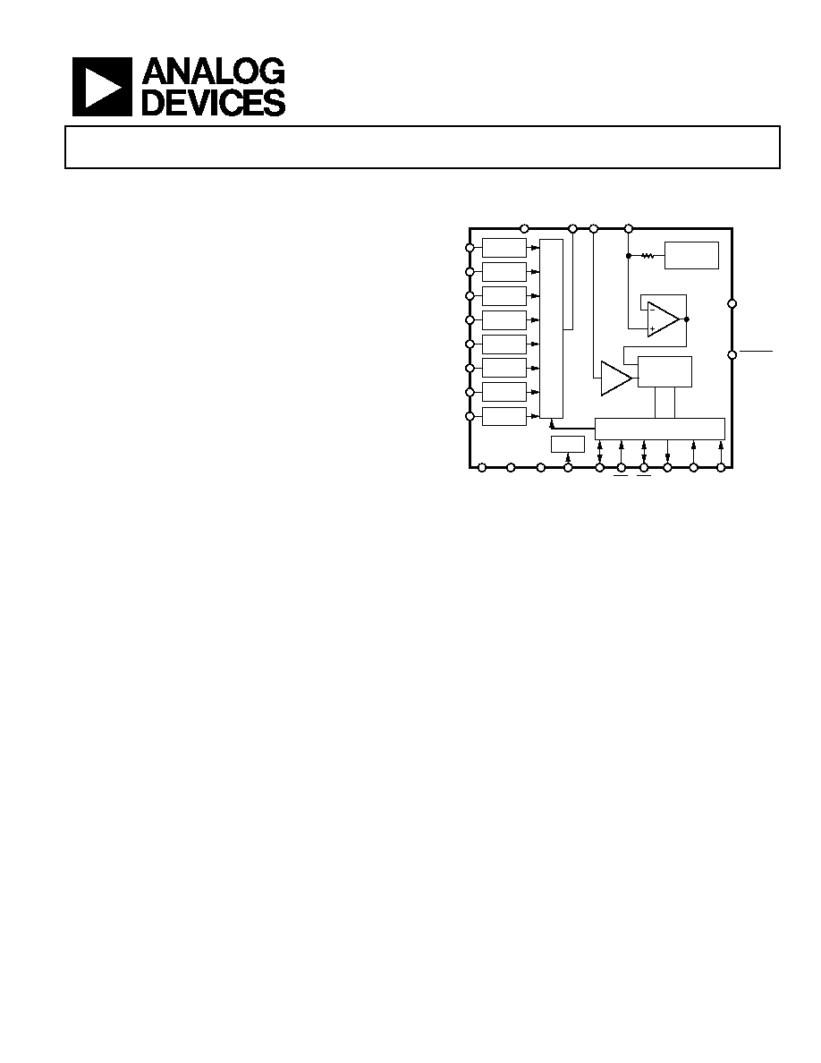
The AD7890 is an 8-channel 12-bit data acquisition system. The
part contains an input multiplexer, an on-chip track/hold
amplifier, a high speed 12-bit ADC, a 2.5 V reference, and a
high speed, serial interface. The part operates from a single 5 V
supply and accepts an analog input range of ±10 V (AD7890-10),
0 V to 4.096 V (AD7890-4), and 0 V to 2.5 V (AD7890-2).
The multiplexer on the part is independently accessible. This
allows the user to insert an antialiasing filter or signal
conditioning, if required, between the multiplexer and the
ADC. This means that one antialiasing filter can be used for all
eight channels. Connection of an external capacitor allows the
user to adjust the time given to the multiplexer settling to
include any external delays in the filter or signal conditioning
circuitry.
Output data from the AD7890 is provided via a high speed
bidirectional serial interface port. The part contains an on-chip
control register, allowing control of channel selection,
conversion start, and power-down via the serial port. Versatile,
high speed logic ensures easy interfacing to serial ports on
microcontrollers and digital signal processors.
In addition to the traditional dc accuracy specifications such as
linearity, full-scale, and offset errors, the AD7890 is also
specified for dynamic performance parameters including
harmonic distortion and signal-to-noise ratio.
FUNCTIONAL BLOCK DIAGRAM
TRACK/HOLD
2k
AD7890
CEXT
CONVST
MUX
OUT
SHA
IN
REF OUT/
REF IN
AGND AGND DGND
SCLK TFS RFS DATA
OUT
DATA
IN
SMODE
VIN1
VDD
VIN2
VIN3
VIN4
VIN5
VIN6
VIN7
VIN8
1NO SCALING ON AD7890-2
CLOCK
OUTPUT/CONTROL REGISTER
12-BIT
ADC
MUX
2.5V
REFERENCE
SIGNAL
SCALING1
SIGNAL
SCALING1
SIGNAL
SCALING1
SIGNAL
SCALING1
SIGNAL
SCALING1
SIGNAL
SCALING1
SIGNAL
SCALING1
SIGNAL
SCALING1
CLK
IN
01
35
7-
00
1
Figure 1.
Power dissipation in normal mode is low at 30 mW typical and the
part can be placed in a standby (power-down) mode if it is not
required to perform conversions. The AD7890 is fabricated in
Analog Devices, Inc.’s Linear Compatible CMOS (LC2MOS)
process, a mixed technology process that combines precision
bipolar circuits with low power CMOS logic. The part is available
in a 24-lead, 0.3" wide, plastic or ceramic dual-in-line package or in
a 24-lead small outline package (SOIC_W).
PRODUCT HIGHLIGHTS
1.
Complete 12-Bit Data Acquisition System-on-a-Chip.
The AD7890 is a complete monolithic ADC combining an
8-channel multiplexer, 12-bit ADC, 2.5 V reference, and a
track/hold amplifier on a single chip.
2.
Separate Access to Multiplexer and ADC.
The AD7890 provides access to the output of the
multiplexer allowing one antialiasing filter for 8 channels—
a considerable savings over the 8 antialiasing filters required if
the multiplexer is internally connected to the ADC.
3.
High Speed Serial Interface.
The part provides a high speed serial interface for easy
connection to serial ports of microcontrollers and DSP
processors.
相关PDF资料 |
PDF描述 |
|---|---|
| LTC6905IS5-96#TRMPBF | IC OSC SILICON 96MHZ TSOT23-5 |
| AD7890BNZ-10 | IC DAS 12BIT 8CH 24-DIP |
| VE-20L-MY-S | CONVERTER MOD DC/DC 28V 50W |
| AD7891BP-2REEL | IC DAS 12BIT 8CH 44-PLCC |
| VE-20K-MY-S | CONVERTER MOD DC/DC 40V 50W |
相关代理商/技术参数 |
参数描述 |
|---|---|
| AD7890BNZ-4 | 功能描述:IC DAS 12BIT 8CH 24-DIP RoHS:是 类别:集成电路 (IC) >> 数据采集 - ADCs/DAC - 专用型 系列:- 产品培训模块:Lead (SnPb) Finish for COTS Obsolescence Mitigation Program 标准包装:50 系列:- 类型:数据采集系统(DAS) 分辨率(位):16 b 采样率(每秒):21.94k 数据接口:MICROWIRE?,QSPI?,串行,SPI? 电压电源:模拟和数字 电源电压:1.8 V ~ 3.6 V 工作温度:-40°C ~ 85°C 安装类型:表面贴装 封装/外壳:40-WFQFN 裸露焊盘 供应商设备封装:40-TQFN-EP(6x6) 包装:托盘 |
| AD7890BR-10 | 功能描述:IC DAS 12BIT 8CH 24-SOIC RoHS:否 类别:集成电路 (IC) >> 数据采集 - ADCs/DAC - 专用型 系列:- 产品培训模块:Lead (SnPb) Finish for COTS Obsolescence Mitigation Program 标准包装:50 系列:- 类型:数据采集系统(DAS) 分辨率(位):16 b 采样率(每秒):21.94k 数据接口:MICROWIRE?,QSPI?,串行,SPI? 电压电源:模拟和数字 电源电压:1.8 V ~ 3.6 V 工作温度:-40°C ~ 85°C 安装类型:表面贴装 封装/外壳:40-WFQFN 裸露焊盘 供应商设备封装:40-TQFN-EP(6x6) 包装:托盘 |
| AD7890BR-10REEL | 功能描述:IC DAS 12BIT 8CH 24-SOIC RoHS:否 类别:集成电路 (IC) >> 数据采集 - ADCs/DAC - 专用型 系列:- 产品培训模块:Lead (SnPb) Finish for COTS Obsolescence Mitigation Program 标准包装:50 系列:- 类型:数据采集系统(DAS) 分辨率(位):16 b 采样率(每秒):21.94k 数据接口:MICROWIRE?,QSPI?,串行,SPI? 电压电源:模拟和数字 电源电压:1.8 V ~ 3.6 V 工作温度:-40°C ~ 85°C 安装类型:表面贴装 封装/外壳:40-WFQFN 裸露焊盘 供应商设备封装:40-TQFN-EP(6x6) 包装:托盘 |
| AD7890BR-2 | 制造商:Analog Devices 功能描述:ADC Single SAR 117ksps 12-bit Serial 24-Pin SOIC W 制造商:Rochester Electronics LLC 功能描述:8-CH,100K,12-BIT ADC - Bulk |
| AD7890BR-2REEL | 制造商:Analog Devices 功能描述:ADC Single SAR 117ksps 12-bit Serial 24-Pin SOIC W T/R |
发布紧急采购,3分钟左右您将得到回复。