参数资料
| 型号: | AD7890BRZ-4 |
| 厂商: | Analog Devices Inc |
| 文件页数: | 6/28页 |
| 文件大小: | 0K |
| 描述: | IC DAS 12BIT 8CH 24-SOIC |
| 产品变化通告: | Product Discontinuance 27/Oct/2011 |
| 标准包装: | 31 |
| 类型: | 数据采集系统(DAS) |
| 分辨率(位): | 12 b |
| 采样率(每秒): | 117k |
| 数据接口: | 串行 |
| 电压电源: | 单电源 |
| 电源电压: | 5V |
| 工作温度: | -40°C ~ 85°C |
| 安装类型: | 表面贴装 |
| 封装/外壳: | 24-SOIC(0.295",7.50mm 宽) |
| 供应商设备封装: | 24-SOIC W |
| 包装: | 管件 |
第1页第2页第3页第4页第5页当前第6页第7页第8页第9页第10页第11页第12页第13页第14页第15页第16页第17页第18页第19页第20页第21页第22页第23页第24页第25页第26页第27页第28页
AD7890
Rev. C | Page 14 of 28
When using the device in the external-clocking mode, the
output register can be read at any time and the most up-to-date
conversion result is obtained. However, reading data from the
output register or writing data to the control register during
conversion or during the 500 ns prior to the next CONVST
results in reduced performance from the part. A read operation
to the output register has the most effect on performance with
the signal-to-noise ratio likely to degrade, especially when
higher serial clock rates are used while the code flicker from the
part also increases (see the Performance section).
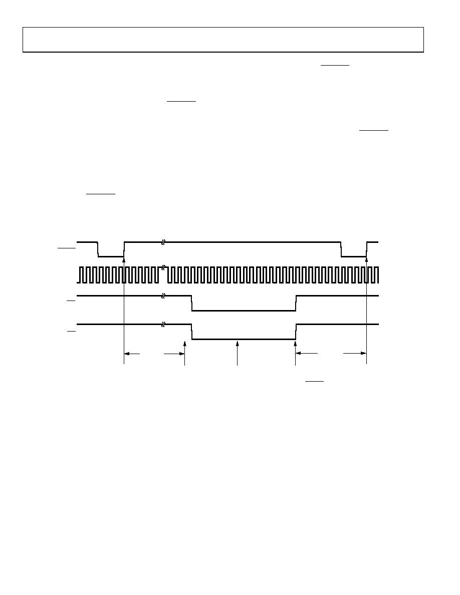
Figure 7 shows the timing and control sequence required to
obtain optimum performance from the part in the external
clocking mode. In the sequence shown, conversion is initiated
on the rising edge of CONVST and new data is available in the
output register of the AD7890 5.9 μs later. Once the read
operation has taken place, a further 500 ns should be allowed
before the next rising edge of CONVST to optimize the settling
of the track/hold before the next conversion is initiated.
The diagram shows the read operation and the write operation
taking place in parallel. On the sixth falling edge of SCLK in the
write sequence the internal pulse is initiated. Assuming MUX OUT
is connected to SHA IN, 2 μs are required between this sixth
falling edge of SCLK and the rising edge of CONVST to allow
for the full acquisition time of the track/hold amplifier. With
the serial clock rate at its maximum of 10 MHz, the achievable
throughput rate for the part is 5.9 μs (conversion time) plus 0.6
μs (six serial clock pulses before internal pulse is initiated) plus
2 μs (acquisition time). This results in a minimum throughput
time of 8.5 μs (equivalent to a throughput rate of 117 kHz). If
the part is operated with a slower serial clock, it affects the
achievable throughput rate for optimum performance.
RFS
TFS
500ns MIN
CONVST
SCLK
NEXT CONVERSION
START COMMAND
CONVERSION IS
INITIATED AND
TRACK/HOLD GOES
INTO HOLD
CONVERSION
ENDS 5.9s
LATER
SERIAL READ
AND WRITE
OPERATIONS
READ AND WRITE
OPERATIONS SHOULD END
500ns PRIOR TO NEXT
RISING EDGE OF CONVST
tCONVERT
01
35
7-
00
7
Figure 7. External Clocking (Slave) Mode Timing Sequence for Optimum Performance
相关PDF资料 |
PDF描述 |
|---|---|
| AD7891BPZ-2 | IC DAS 12BIT 8CH 44-PLCC |
| AD80066KRSZRL | IC DSP CTLR 16BIT 28SSOP |
| AD8016AREZ-REEL7 | IC LINE DRIVER ADSL 28TSSOP |
| AD8018ARZ | IC XDSL LINE DVR R-R 8-SOIC |
| AD807A-155BR | IC FIBER OPTIC RCVR 16-SOIC |
相关代理商/技术参数 |
参数描述 |
|---|---|
| AD7890BRZ-4REEL | 功能描述:IC DAS 12BIT 8CH 24-SOIC RoHS:是 类别:集成电路 (IC) >> 数据采集 - ADCs/DAC - 专用型 系列:- 产品培训模块:Lead (SnPb) Finish for COTS Obsolescence Mitigation Program 标准包装:50 系列:- 类型:数据采集系统(DAS) 分辨率(位):16 b 采样率(每秒):21.94k 数据接口:MICROWIRE?,QSPI?,串行,SPI? 电压电源:模拟和数字 电源电压:1.8 V ~ 3.6 V 工作温度:-40°C ~ 85°C 安装类型:表面贴装 封装/外壳:40-WFQFN 裸露焊盘 供应商设备封装:40-TQFN-EP(6x6) 包装:托盘 |
| AD7890SQ-10 | 功能描述:模数转换器 - ADC LC2MOS 8CH 12B Data Acquisition System RoHS:否 制造商:Analog Devices 通道数量: 结构: 转换速率: 分辨率: 输入类型: 信噪比: 接口类型: 工作电源电压: 最大工作温度: 安装风格: 封装 / 箱体: |
| AD7890SQ-2 | 功能描述:模数转换器 - ADC LC2MOS 8CH 12B Data Acquisition System RoHS:否 制造商:Analog Devices 通道数量: 结构: 转换速率: 分辨率: 输入类型: 信噪比: 接口类型: 工作电源电压: 最大工作温度: 安装风格: 封装 / 箱体: |
| AD7890SQ-4 | 功能描述:模数转换器 - ADC LC2MOS 8CH 12B Data Acquisition System RoHS:否 制造商:Analog Devices 通道数量: 结构: 转换速率: 分辨率: 输入类型: 信噪比: 接口类型: 工作电源电压: 最大工作温度: 安装风格: 封装 / 箱体: |
| AD7891AP1 | 制造商:Analog Devices 功能描述: |
发布紧急采购,3分钟左右您将得到回复。