参数资料
| 型号: | AD7891YPZ-1REEL |
| 厂商: | Analog Devices Inc |
| 文件页数: | 4/20页 |
| 文件大小: | 0K |
| 描述: | IC DAS 12BIT 8CH 44-PLCC |
| 产品变化通告: | Product Discontinuance 27/Oct/2011 |
| 标准包装: | 500 |
| 类型: | 数据采集系统(DAS) |
| 分辨率(位): | 12 b |
| 采样率(每秒): | 500k |
| 数据接口: | 串行,并联 |
| 电压电源: | 单电源 |
| 电源电压: | 5V |
| 工作温度: | -55°C ~ 105°C |
| 安装类型: | 表面贴装 |
| 封装/外壳: | 44-LCC(J 形引线) |
| 供应商设备封装: | 44-PLCC(16.59x16.59) |
| 包装: | 带卷 (TR) |
AD7891
–12–
REV. D
CIRCUIT DESCRIPTION
Reference
The AD7891 contains a single reference pin labeled REF OUT/
REF IN that either provides access to the part’s own 2.5 V
internal reference or to which an external 2.5 V reference can be
connected to provide the reference source for the part. The part
is specified with a 2.5 V reference voltage. Errors in the reference
source result in gain errors in the transfer function of the AD7891
and add to the specified full-scale errors on the part. They also
result in an offset error injected into the attenuator stage.
The AD7891 contains an on-chip 2.5 V reference. To use this
reference as a reference source for the AD7891, simply connect
a 0.1
mF disc ceramic capacitor from the REF OUT/REF IN pin
to REFGND. REFGND should be connected to AGND or the
analog ground plane. The voltage that appears at the REF OUT/
REF IN pin is internally buffered before being applied to the
ADC. If this reference is required for use external to the AD7891,
it should be buffered since the part has a FET switch in series
with the reference, resulting in a source impedance for this
output of 2 k
W nominal. The tolerance of the internal reference
is
±10 mV at 25∞C with a typical temperature coefficient of
25 ppm/
∞C and a maximum error over temperature of ±20 mV.
If the application requires a reference with a tighter tolerance
or if the AD7891 needs to be used with a system reference, an
external reference can be connected to the REF OUT/REF IN
pin. The external reference overdrives the internal reference
and thus provides the reference source for the ADC. The refer-
ence input is buffered before being applied to the ADC and
the maximum input current is
±100 mA. Suitable reference for
the AD7891 include the AD580, the AD680, the AD780, and
the REF43 precision 2.5 V references.
Analog Input Section
The AD7891 is offered as two part types: the AD7891-1 where
each input can be configured to have a
±10 V or a ±5 V input
range, and the AD7891-2 where each input can be configured
to have a 0 V to +2.5 V, 0 V to +5 V, and
±2.5 V input range.
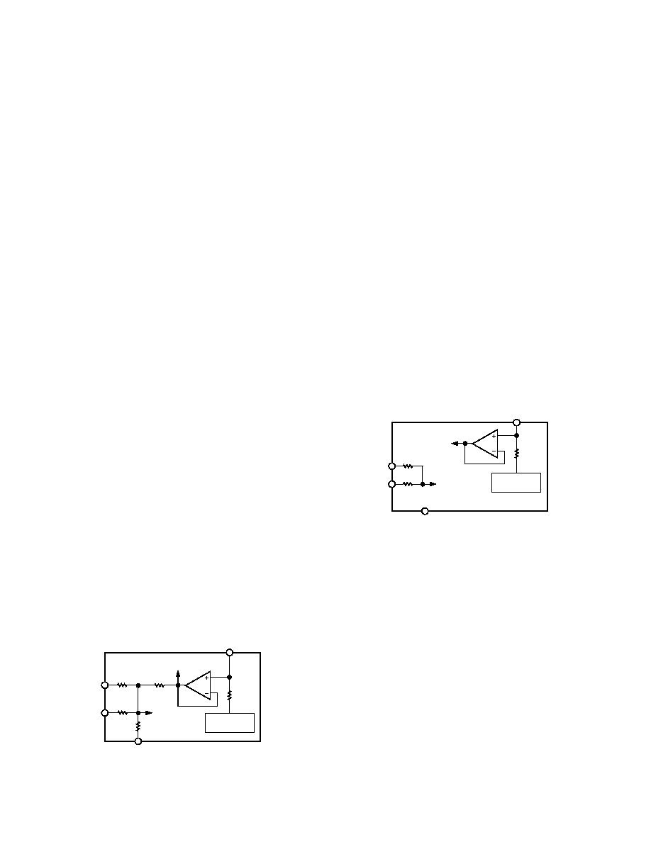
AD7891-1
Figure 5 shows the analog input section of the AD7891-1. Each
input can be configured for
±5 V or ±10 V operation. For 5 V
operation, the VINXA and VINXB inputs are tied together and the
input voltage is applied to both. For
±10 V operation, the VINXB
input is tied to AGND and the input voltage is applied to the
VINXA input. The VINXA and VINXB inputs are symmetrical and
fully interchangeable. Therefore, for ease of PCB layout on the
±10 V range, the input voltage may be applied to the VINXB
input while the VINXA input is tied to AGND.
30k
VINXA
VINXB
AGND
TO
MULTIPLEXER
AD7891-1
2k
REF OUT/REF IN
TO ADC
REFERENCE CIRCUITRY
7.5k
30k
15k
2.5V
REFERENCE
Figure 5. AD7891-1 Analog Input Structure
The input resistance for the
±5 V range is typically 20 kW. For
the
±10 V input range, the input resistance is typically 34.3 kW.
The resistor input stage is followed by the multiplexer, which is
followed by the high input impedance stage of the track/hold
amplifier.
The designed code transitions take place midway between suc-
cessive integer LSB values (i.e., 1/2 LSB, 3/2 LSBs, 5/2 LSBs).
LSB size is given by the formula 1 LSB = FS/4096. Therefore, for
the
±5 V range, 1 LSB = 10 V/4096 = 2.44 mV. For the ±10 V
range, 1 LSB = 20 V/4096 = 4.88 mV. Output coding is deter-
mined by the FORMAT bit of the control register. The ideal
input/output code transitions are shown in Table I.
AD7891-2
Figure 6 shows the analog input section of the AD7891-2. Each
input can be configured for input ranges of 0 V to +5 V, 0 V to +2.5 V,
or
±2.5 V. For the 0 V to 5 V input range, the VINXB input is
tied to AGND and the input voltage is applied to the VINXA input.
For the 0 V to 2.5 V input range, the VINXA and VINXB inputs
are tied together and the input voltage is applied to both. For
the
±2.5 V input range, the VINXB input is tied to 2.5 V and
the input voltage is applied to the VINXA input. The 2.5 V source
must have a low output impedance. If the internal reference on
the AD7891 is used, it must be buffered before being applied to
VINXB. The VINXA and VINXB inputs are symmetrical and fully
interchangeable. Therefore, for ease of PCB layout on the 0 V to +5 V
or
±2.5 V range, the input voltage may be applied to the VINXB
input, while the VINXA input is tied to AGND or 2.5 V.
1.8k
VINXA
VINXB
AGND
TO
MULTIPLEXER
AD7891-2
2k
REF OUT/REF IN
TO ADC
REFERENCE
CIRCUITRY
1.8k
2.5V
REFERENCE
Figure 6. AD7891-2 Analog Input Structure
The input resistance for both the 0 V to +5 V and
±2.5 V ranges
is typically 3.6 k
W. When an input is configured for 0 V to 2.5 V
operation, the input is fed into the high impedance stage of the
track/hold amplifier via the multiplexer and the two 1.8 k
W
resistors in parallel.
The designed code transitions occur midway between successive
integer LSB values (i.e., 1/2 LSB, 3/2 LSBs, 5/2 LSBs). LSB size
is given by the formula 1 LSB = FS/4096. Therefore, for the 0 V
to 5 V range, 1 LSB = 5 V/4096 = 1.22 mV, for the 0 V to 2.5 V
range, 1 LSB = 2.5 V/4096 = 0.61 mV, and for the
±2.5 V range,
1 LSB = 5 V/4096 = 1.22 mV. Output coding is determined by
the FORMAT bit in the control register. The ideal input/output
code transitions for the
±2.5 V range are shown in Table I. The
ideal input/output code transitions for the 0 V to 5 V range and
the 0 V to 2.5 V range are shown in Table II.
相关PDF资料 |
PDF描述 |
|---|---|
| MS27473E22F35PA | CONN PLUG 100POS STRAIGHT W/PINS |
| LTC1296DISW#TRPBF | IC DATA ACQ SYSTEM 12BIT 20-SOIC |
| LTC1289BCN#PBF | IC DATA ACQ SYS 12BIT 3V 20-DIP |
| MS27467T25F35PD | CONN PLUG 128POS STRAIGHT W/PINS |
| MS3456W18-10P | CONN PLUG 4POS STRAIGHT W/PINS |
相关代理商/技术参数 |
参数描述 |
|---|---|
| AD7891YS1 | 制造商:AD 功能描述:New |
| AD7891YS-1 | 制造商:Analog Devices 功能描述:ADC Single 454.5ksps 12-bit Parallel/Serial 44-Pin MQFP |
| AD7891YS-1REEL | 制造商:Analog Devices 功能描述:ADC Single 454.5ksps 12-bit Parallel/Serial 44-Pin MQFP T/R 制造商:Analog Devices 功能描述:ADC SGL 454.5KSPS 12-BIT PARALLEL/SERL 44MQFP - Tape and Reel |
| AD7891YS-2 | 制造商:Analog Devices 功能描述:ADC Single 500ksps 12-bit Parallel/Serial 44-Pin MQFP 制造商:Rochester Electronics LLC 功能描述:8 CHANNEL, 12-BIT ADC I.C. - Bulk |
| AD7891YS-2REEL | 制造商:Analog Devices 功能描述:ADC Single 500ksps 12-bit Parallel/Serial 44-Pin MQFP T/R |
发布紧急采购,3分钟左右您将得到回复。