- 您现在的位置:买卖IC网 > PDF目录10121 > AD7893BR-2 (Analog Devices Inc)IC ADC 12BIT SRL T/H LP 8-SOIC PDF资料下载
参数资料
| 型号: | AD7893BR-2 |
| 厂商: | Analog Devices Inc |
| 文件页数: | 7/12页 |
| 文件大小: | 0K |
| 描述: | IC ADC 12BIT SRL T/H LP 8-SOIC |
| 标准包装: | 1 |
| 位数: | 12 |
| 采样率(每秒): | 117k |
| 数据接口: | 串行 |
| 转换器数目: | 1 |
| 功率耗散(最大): | 45mW |
| 电压电源: | 单电源 |
| 工作温度: | -40°C ~ 85°C |
| 安装类型: | 表面贴装 |
| 封装/外壳: | 8-SOIC(0.154",3.90mm 宽) |
| 供应商设备封装: | 8-SOIC |
| 包装: | 管件 |
| 输入数目和类型: | 1 个单端,单极 |
AD7893
REV. E
–4–
PIN FUNCTION DESCRIPTION
Pin
No.
Mnemonic
Description
1
REF IN
Voltage Reference Input. An external reference source should be connected to this pin to provide the refer-
ence voltage for the AD7893’s conversion process. The REF IN input is buffered on-chip. The nominal ref-
erence voltage for correct operation of the AD7893 is +2.5 V.
2VIN
Analog Input Channel. The analog input range is
±10 V (AD7893-10), ±2.5 V (AD7893-3), 0 V to +5 V
(AD7893-5) and 0 V to +2.5 V (AD7893-2).
3
AGND
Analog Ground. Ground reference for track/hold, comparator and DAC.
4
SCLK
Serial Clock Input. An external serial clock is applied to this input to obtain serial data from the AD7893. A
new serial data bit is clocked out on the rising edge of this serial clock, and data is valid on the falling edge.
The serial clock input should be taken low at the end of the serial data transmission.
5
SDATA
Serial Data Output. Serial data from the AD7893 is provided at this output. The serial data is clocked out by
the rising edge of SCLK and is valid on the falling edge of SCLK. Sixteen bits of serial data are provided
with four leading zeros followed by the 12 bits of conversion data. On the sixteenth falling edge of SCLK, the
SDATA line is disabled (three-stated). Output data coding is twos complement for the AD7893-10 and
AD7893-3, straight binary for the AD7893-2 and AD7893-5.
6
DGND
Digital Ground. Ground reference for digital circuitry.
7
CONVST
Convert Start. Edge-triggered logic input. On the falling edge of this input, the serial clock counter is reset to
zero. On the rising edge of this input, the track/hold goes into its hold mode and conversion is initiated.
8VDD
Positive supply voltage, +5 V
± 5%.
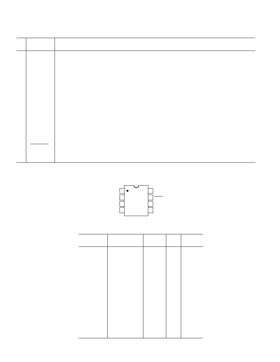
PIN CONFIGURATION
DIP and SOIC
1
2
3
4
8
7
6
5
REF IN
VIN
AGND
SCLK
DGND
SDATA
VDD
CONVST
AD7893
TOP VIEW
(NOT TO SCALE)
ORDERING GUIDE
Temperature
Linearity
Package
Model
Range
Error
SNR
Options*
AD7893AN-2
–40
°C to +85°C
±1 LSB
70 dB
N-8
AD7893BN-2
–40
°C to +85°C
±1/2 LSB 72 dB N-8
AD7893AR-2
–40
°C to +85°C
±1 LSB
70 dB
SO-8
AD7893BR-2
–40
°C to +85°C
±1/2 LSB 72 dB SO-8
AD7893SQ-2
–55
°C to +125°C ±1 LSB
70 dB
Q-8
AD7893AN-5
–40
°C to +85°C
±1 LSB
70 dB
N-8
AD7893BN-5
–40
°C to +85°C
±1/2 LSB 72 dB N-8
AD7893AR-5
–40
°C to +85°C
±1 LSB
70 dB
SO-8
AD7893BR-5
–40
°C to +85°C
±1/2 LSB 72 dB SO-8
AD7893SQ-5
–55
°C to +125°C ±1 LSB
70 dB
Q-8
AD7893AN-10 –40
°C to +85°C
±1 LSB
70 dB
N-8
AD7893BN-10 –40
°C to +85°C
±1/2 LSB 72 dB N-8
AD7893AR-10
–40
°C to +85°C
±1 LSB
70 dB
SO-8
AD7893BR-10
–40
°C to +85°C
±1/2 LSB 72 dB SO-8
AD7893SQ-10
–55
°C to +125°C ±1 LSB
70 dB
Q-8
AD7893AR-3
–40
°C to +85°C
±1 LSB
70 dB
SO-8
*N = Plastic DIP, Q = Cerdip, SO = SOIC.
相关PDF资料 |
PDF描述 |
|---|---|
| IDT72421L10PF8 | IC FIFO 64X9 SYNC 10NS 32-TQFP |
| MS27508E20A35P | CONN RCPT 79POS BOX MNT W/PINS |
| VI-23Z-IU-F2 | CONVERTER MOD DC/DC 2V 80W |
| LTC1605AIG#TRPBF | IC A/D CONV 16BIT SAMPLNG 28SSOP |
| VI-23Z-IU-F1 | CONVERTER MOD DC/DC 2V 80W |
相关代理商/技术参数 |
参数描述 |
|---|---|
| AD7893BR-2REEL | 制造商:Analog Devices 功能描述:ADC Single SAR 117ksps 12-bit Serial 8-Pin SOIC N T/R 制造商:Analog Devices 功能描述:ADC SGL SAR 117KSPS 12-BIT SERL 8SOIC N - Tape and Reel |
| AD7893BR-2REEL7 | 功能描述:IC ADC 12BIT SRL T/H LP 8-SOIC RoHS:否 类别:集成电路 (IC) >> 数据采集 - 模数转换器 系列:- 标准包装:1,000 系列:- 位数:12 采样率(每秒):300k 数据接口:并联 转换器数目:1 功率耗散(最大):75mW 电压电源:单电源 工作温度:0°C ~ 70°C 安装类型:表面贴装 封装/外壳:24-SOIC(0.295",7.50mm 宽) 供应商设备封装:24-SOIC 包装:带卷 (TR) 输入数目和类型:1 个单端,单极;1 个单端,双极 |
| AD7893BR-5 | 制造商:Analog Devices 功能描述:ADC SGL SAR 117KSPS 12-BIT SERL 8SOIC N - Rail/Tube 制造商:Rochester Electronics LLC 功能描述:12-BIT ADC,8-PIN I.C. - Bulk |
| AD7893BR-5REEL | 制造商:Analog Devices 功能描述:ADC SGL SAR 117KSPS 12-BIT SERL 8SOIC N - Tape and Reel |
| AD7893BR-5REEL7 | 制造商:Analog Devices 功能描述: 制造商:Rochester Electronics LLC 功能描述:12-BIT ADC,8-PIN I.C. - Tape and Reel |
发布紧急采购,3分钟左右您将得到回复。