- 您现在的位置:买卖IC网 > PDF目录10231 > AD7894AR-10REEL7 (Analog Devices Inc)IC ADC 14BIT SRL T/H LP 8-SOIC PDF资料下载
参数资料
| 型号: | AD7894AR-10REEL7 |
| 厂商: | Analog Devices Inc |
| 文件页数: | 2/12页 |
| 文件大小: | 0K |
| 描述: | IC ADC 14BIT SRL T/H LP 8-SOIC |
| 标准包装: | 1,000 |
| 位数: | 14 |
| 采样率(每秒): | 200k |
| 数据接口: | 串行 |
| 转换器数目: | 1 |
| 功率耗散(最大): | 27.5mW |
| 电压电源: | 单电源 |
| 工作温度: | -40°C ~ 85°C |
| 安装类型: | 表面贴装 |
| 封装/外壳: | 8-SOIC(0.154",3.90mm 宽) |
| 供应商设备封装: | 8-SOIC |
| 包装: | 带卷 (TR) |
| 输入数目和类型: | 1 个单端,双极 |
AD7894
–10–
REV. 0
AD7894 to ADSP-2101/5 Interface
An interface circuit between the AD7894 and the ADSP-2101/5
DSP processor is shown in Figure 8. In the interface shown, the
RFS1 output from the ADSP-2101/5s SPORT1 serial port is
used to gate the serial clock (SCLK1) of the ADSP-2101/5
before it is applied to the SCLK input of the AD7894. The
RFS1 output is configured for active high operation. The BUSY
line from the AD7894 is connected to the
IRQ2 line of the
ADSP-2101/5 so that at the end of conversion an interrupt is
generated telling the ADSP-2101/5 to initiate a read operation.
The interface ensures a noncontinuous clock for the AD7894’s
serial clock input, with only 16 serial clock pulses provided and
the serial clock line of the AD7894 remaining low between data
transfers. The SDATA line from the AD7894 is connected to
the DR1 line of the ADSP-2101/5’s serial port.
The timing relationship between the SCLK1 and RFS1 outputs
of the ADSP-2101/5 are such that the delay between the rising
edge of the SCLK1 and the rising edge of an active high RFS1
is up to 30 ns. There is also a requirement that data must be set
up 10 ns prior to the falling edge of the SCLK1 to be read cor-
rectly by the ADSP-2101/5. The data access time for the AD7894
is 60 ns (A, B versions) from the rising edge of its SCLK input.
Assuming a 10 ns propagation delay through the external AND
gate, the high time of the SCLK1 output of the ADSP-2105
must be
≥ (30 + 60 + 10 + 10) ns, i.e., ≥ 110 ns. This means
that the serial clock frequency with which the interface of Figure
8 can work is limited to 4.5 MHz.
Another alternative scheme is to configure the ADSP-2101/5
such that it accepts an external noncontinuous serial clock. In
this case, an external noncontinuous serial clock is provided that
drives the serial clock inputs of both the ADSP-2101/5 and the
AD7894. In this scheme, the serial clock frequency is limited to
the processor’s cycle rate, up to a maximum of 13.8 MHz.
IRQ2
SCLK1
DR1
SDATA
BUSY
AD7894
ADSP-2101/5
SCLK
RFS1
Figure 8. AD7894 to ADSP-2101/5 Interface
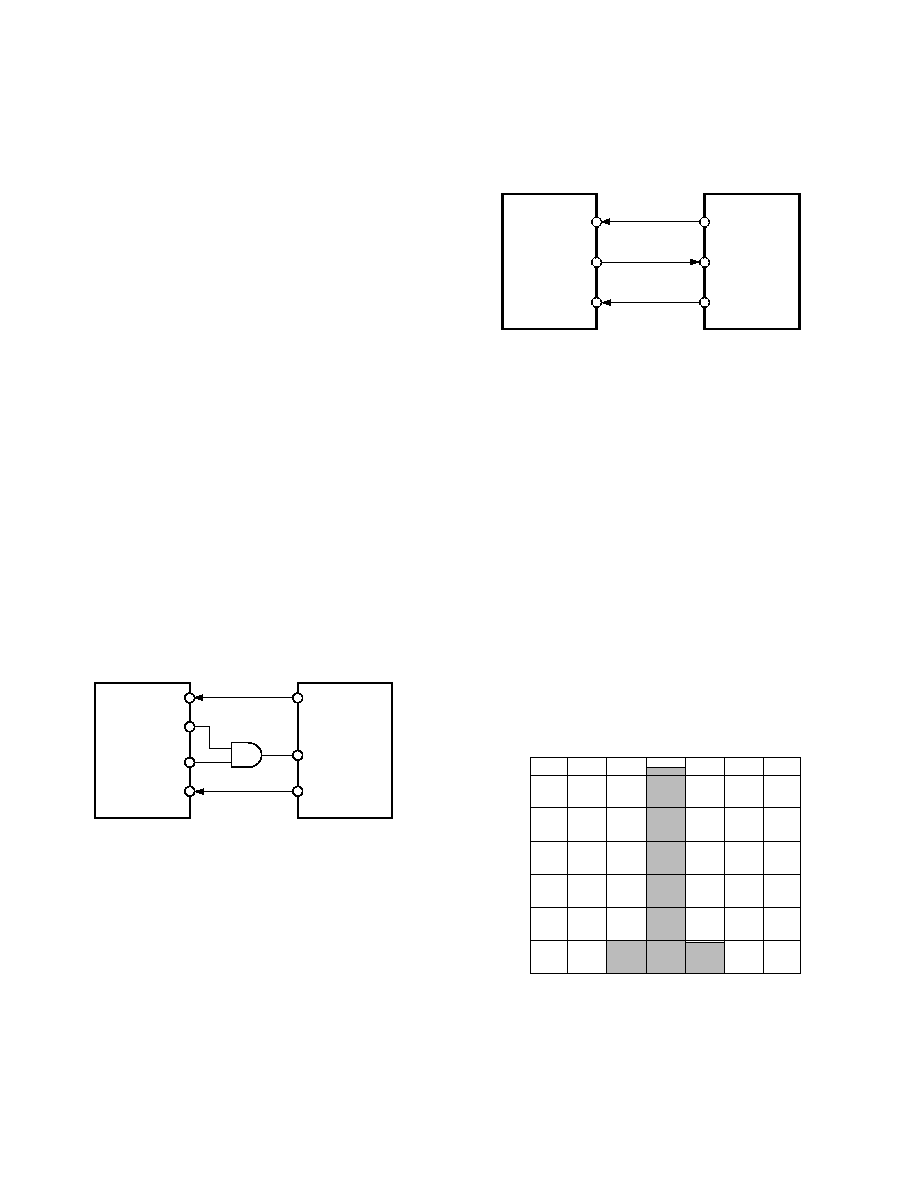
AD7894 to DSP56002/L002 Interface
Figure 9 shows an interface circuit between the AD7894 and the
DSP56002/L002 DSP processor. The DSP56002/L002 is
configured for normal-mode asynchronous operation with gated
clock. It is also set up for a 16-bit word with SCK as gated
clock output. In this mode, the DSP56002/L002 provides 16
serial clock pulses to the AD7894 in a serial read operation.
The DSP56002/L002 assumes valid data on the first falling
edge of SCK so the interface is simply three-wire as shown in
Figure 9.
The BUSY line from the AD7894 is connected to the MODA/
IRQA input of the DSP56002/L002 so that an interrupt will be
generated at the end of conversion. This ensures that the read
operation will take place after conversion is finished.
MODA/
IRQA
SCK
SDR
SDATA
BUSY
SCLK
AD7894
DSP56002/L002
Figure 9. AD7894 to DSP56002/L002 Interface
AD7894 PERFORMANCE
Linearity
The linearity of the AD7894 is determined by the on-chip
14-bit D/A converter. This is a segmented DAC which is laser
trimmed for 14-bit integral linearity and differential linearity.
Typical relative accuracy numbers for the part are
±1/2 LSB
while the typical DNL errors are
±1/3 LSB.
Noise
In an A/D converter, noise exhibits itself as code uncertainty in
dc applications and as the noise floor (in an FFT, for example)
in ac applications. In a sampling A/D converter like the AD7894,
all information about the analog input appears in the baseband
from dc to 1/2 the sampling frequency. The input bandwidth of
the track/hold exceeds the Nyquist bandwidth, so an antialiasing
filter should be used to remove unwanted signals above fS/2 in
the input signal in applications where such signals exist.
Figure 10 shows a histogram plot for 8192 conversions of a dc
input using the AD7894. The analog input was set at the center
of a code transition. It can be seen that almost all the codes
appear in the one output bin indicating very good noise perfor-
mance from the ADC.
ADC CODE
6000
0
103
97
COUNTS
98
99
100
101
102
5000
4000
3000
2000
1000
Figure 10. Histogram of 8192 Conversions of a DC Input
相关PDF资料 |
PDF描述 |
|---|---|
| VI-BNY-IU-S | CONVERTER MOD DC/DC 3.3V 132W |
| VE-J1M-MX-S | CONVERTER MINIMOD DC/DC 10V 75W |
| VI-22L-MX-F4 | CONVERTER MOD DC/DC 28V 75W |
| VI-B3T-IV-S | CONVERTER MOD DC/DC 6.5V 150W |
| AD7858LBR-REEL | IC ADC 12BIT 8CH SRL 24-SOIC |
相关代理商/技术参数 |
参数描述 |
|---|---|
| AD7894AR-10Z | 制造商:Analog Devices 功能描述:ADC 14BIT 5V 7.5MHZ 2LSB 制造商:Analog Devices 功能描述:ADC, 14BIT, 5V, 7.5MHZ, 2LSB, 8SOIC; Resolution (Bits):14bit; Sampling Rate:200kSPS; Supply Voltage Type:Single; Supply Voltage Min:4.75V; Supply Voltage Max:5.25V; Supply Current:5.5mA; Digital IC Case Style:NSOIC; No. of Pins:8; ;RoHS Compliant: Yes |
| AD7894AR-2 | 制造商:Analog Devices 功能描述:ADC Single SAR 200ksps 14-bit Serial 8-Pin SOIC N 制造商:Analog Devices 功能描述:CONVERTOR AD ((NW)) |
| AD7894AR-2REEL | 制造商:Analog Devices 功能描述:ADC Single SAR 200ksps 14-bit Serial 8-Pin SOIC N T/R 制造商:Analog Devices 功能描述:ADC SGL SAR 200KSPS 14BIT SERL 8SOIC N - Tape and Reel |
| AD7894AR-2REEL7 | 制造商:Analog Devices 功能描述:ADC Single SAR 200ksps 14-bit Serial 8-Pin SOIC N T/R |
| AD7894AR-2Z | 制造商:Analog Devices 功能描述:ADC 14BIT 5V 7.5MHZ 2LSB 制造商:Analog Devices 功能描述:ADC, 14BIT, 5V, 7.5MHZ, 2LSB, 8SOIC; Resolution (Bits):14bit; Sampling Rate:200kSPS; Supply Voltage Type:Single; Supply Voltage Min:4.75V; Supply Voltage Max:5.25V; Supply Current:5.5mA; Digital IC Case Style:NSOIC; No. of Pins:8; ;RoHS Compliant: Yes |
发布紧急采购,3分钟左右您将得到回复。