- 您现在的位置:买卖IC网 > PDF目录10225 > AD7895BRZ-2 (Analog Devices Inc)IC ADC 12BIT SRL 5V 8SOIC PDF资料下载
参数资料
| 型号: | AD7895BRZ-2 |
| 厂商: | Analog Devices Inc |
| 文件页数: | 11/12页 |
| 文件大小: | 0K |
| 描述: | IC ADC 12BIT SRL 5V 8SOIC |
| 标准包装: | 1 |
| 位数: | 12 |
| 采样率(每秒): | 192k |
| 数据接口: | 串行 |
| 转换器数目: | 1 |
| 功率耗散(最大): | 20mW |
| 电压电源: | 单电源 |
| 工作温度: | -40°C ~ 85°C |
| 安装类型: | 表面贴装 |
| 封装/外壳: | 8-SOIC(0.154",3.90mm 宽) |
| 供应商设备封装: | 8-SOIC |
| 包装: | 管件 |
| 输入数目和类型: | 1 个单端,单极 |
AD7895
–8–
REV. 0
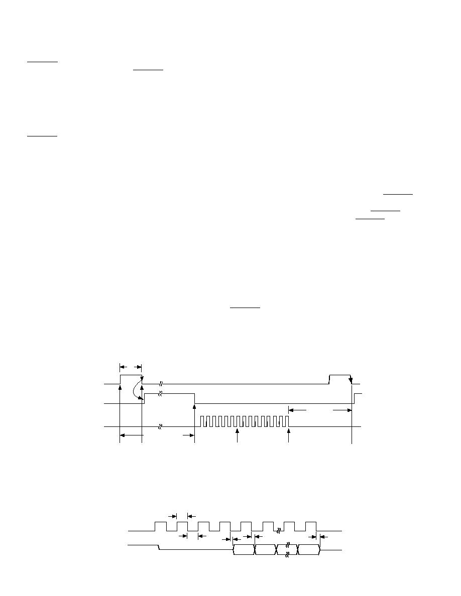
than the 9.8
s shown in diagram from the rising edge of
CONVST
. This is because the Track/Hold amplifier goes into
its hold mode on the falling edge of CONVST, and the conver-
sion will not be complete for a further 3.8
s. In this case, the
BUSY will be the best indicator for when the conversion is
complete. Even though the part is in sleep mode, data can still
be read from the part. The read operation consists of 16 clock
cycles as in Mode 1 Operation. For the fastest serial clock of
15 MHz, the read operation will take 1.1
s and this must be
complete at least 300 ns before the falling edge of the next
CONVST
to allow the Track/Hold amplifier to have enough
time to settle. This mode is very useful when the part is convert-
ing at a slow rate as the power consumption will be significantly
reduced from that of Mode 1 Operation.
Serial Interface
The serial interface to the AD7895 consists of just three wires: a
serial clock input (SCLK), the serial data output (SDATA) and
a conversion status output (BUSY). This allows for an easy-to-
use interface to most microcontrollers, DSP processors and shift
registers.
Figure 5 shows the timing diagram for the read operation to the
AD7895. The serial clock input (SCLK) provides the clock
source for the serial interface. Serial data is clocked out from the
SDATA line on the falling edge of this clock and is valid on
both the rising and falling edges of SCLK. The advantage of
having the data valid on both the rising and falling edges of the
SCLK is that it gives the user greater flexibility in interfacing to
the part and allows a wider range of microprocessor and micro-
controller interfaces to be accommodated. This also explains the
two timing figures, t4 and t5, that are quoted on the diagram.
The time t4 specifies how long after the falling edge of the
SCLK that the next data bit becomes valid, whereas the time t5
specifies how long after the falling edge of the SCLK that the
current data bit is valid for. The first leading zero is clocked out
on the first rising edge of SCLK. Note that the first zero will be
valid on the first falling edge of SCLK even though the data
access time is specified at 60 ns for the other bits. The reason
that the first bit will be clocked out faster than the other bits is
due to the internal architecture of the part. Sixteen clock pulses
must be provided to the part to access to full conversion result.
The AD7895 provides four leading zeros, followed by the 12-bit
conversion result starting with the MSB (DB11). The last data
bit to be clocked out on the penultimate falling clock edge is the
LSB (DB0). On the sixteenth falling edge of SCLK, the LSB
(DB0) will be valid for a specified time to allow the bit to be
read on the falling edge of the SCLK, then the SDATA line is
disabled (three-stated). After this last bit has been clocked
out, the SCLK input should return low and remain low until the
next serial data read operation. If there are extra clock pulses
after the sixteenth clock, the AD7895 will start over again with
outputting data from its output register, and the data bus will no
longer be three-stated even when the clock stops. Provided the
serial clock has stopped before the next falling edge of CONVST,
the AD7895 will continue to operate correctly with the output
shift register being reset on the falling edge of CONVST.
However, the SCLK line must be low when CONVST goes low in
order to reset the output shift register correctly.
The serial clock input does not have to be continuous during the
serial read operation. The sixteen bits of data (four leading
zeros and 12 bit conversion result) can be read from the AD7895
in a number of bytes.
The AD7895 counts the serial clock edges to know which bit
from the output register should be placed on the SDATA
output. To ensure that the part does not lose synchronization,
the serial clock counter is reset on the falling edge of the
CONVST
input, provided the SCLK line is low. The user
should ensure that the SCLK line remains low until the end of
the conversion. When the conversion is complete, BUSY goes
low, the output register will be loaded with the new conversion
result and can be read from with sixteen clock cycles of SCLK.
CONVST
BUSY
SCLK
SERIAL READ
OPERATION
CONVERSION
ENDS
9.8s LATER
READ OPERATION
SHOULD END 300ns
PRIOR TO NEXT
FALLING EDGE OF
CONVST
OUTPUT
SERIAL
SHIFT
REGISTER
IS RESET
PART
WAKES
UP
CONVERSION
IS INITIATED
TRACK/HOLD
GOES INTO
HOLD
t1 = 6s
WAKE-UP
TIME
t
1
tCONVERT = 9.8s
300ns MIN
Figure 4. Mode 2 Timing Diagram Where Automatic Sleep Function Is Initiated
t2
4 LEADING ZEROS
DOUT (O/P)
SCLK (I/P)
t6
1
2
3
4
5
6
15
16
DB0
DB10
DB11
3-STATE
t5
t3
t4
3-STATE
t2 = t3 = 35ns MIN, t4 = 60ns MAX, t5 = 10ns MIN, t6 = 50ns MAX @ 5V, A, B, VERSIONS
Figure 5. Data Read Operation
相关PDF资料 |
PDF描述 |
|---|---|
| MS3101E28-17P | CONN RCPT 15POS FREE HNG W/PINS |
| LTC1409ISW#TR | IC ADC 12BIT 800KSPS SMPL 28SOIC |
| SP490EEN-L/TR | IC TXRX RS485 FULL DUPLEX 8NSOIC |
| MS27467T11A98PA | CONN PLUG 6POS STRAIGHT W/PINS |
| LTC1415ISW#TR | IC ADC 12BIT 1.25MSPS SMP 28SOIC |
相关代理商/技术参数 |
参数描述 |
|---|---|
| AD7896AN | 功能描述:IC ADC 12BIT SRL T/H HS 8-DIP RoHS:否 类别:集成电路 (IC) >> 数据采集 - 模数转换器 系列:- 产品培训模块:Lead (SnPb) Finish for COTS Obsolescence Mitigation Program 标准包装:2,500 系列:- 位数:12 采样率(每秒):3M 数据接口:- 转换器数目:- 功率耗散(最大):- 电压电源:- 工作温度:- 安装类型:表面贴装 封装/外壳:SOT-23-6 供应商设备封装:SOT-23-6 包装:带卷 (TR) 输入数目和类型:- |
| AD7896ANZ | 功能描述:IC ADC 12BIT SRL T/H HS 8DIP RoHS:是 类别:集成电路 (IC) >> 数据采集 - 模数转换器 系列:- 标准包装:1,000 系列:- 位数:12 采样率(每秒):300k 数据接口:并联 转换器数目:1 功率耗散(最大):75mW 电压电源:单电源 工作温度:0°C ~ 70°C 安装类型:表面贴装 封装/外壳:24-SOIC(0.295",7.50mm 宽) 供应商设备封装:24-SOIC 包装:带卷 (TR) 输入数目和类型:1 个单端,单极;1 个单端,双极 |
| AD7896AR | 功能描述:IC ADC 12BIT SRL T/H HS 8-SOIC RoHS:否 类别:集成电路 (IC) >> 数据采集 - 模数转换器 系列:- 标准包装:1,000 系列:- 位数:12 采样率(每秒):300k 数据接口:并联 转换器数目:1 功率耗散(最大):75mW 电压电源:单电源 工作温度:0°C ~ 70°C 安装类型:表面贴装 封装/外壳:24-SOIC(0.295",7.50mm 宽) 供应商设备封装:24-SOIC 包装:带卷 (TR) 输入数目和类型:1 个单端,单极;1 个单端,双极 |
| AD7896AR-REEL | 功能描述:IC ADC 12BIT SRL T/H HS 8-SOIC RoHS:否 类别:集成电路 (IC) >> 数据采集 - 模数转换器 系列:- 标准包装:1,000 系列:- 位数:12 采样率(每秒):300k 数据接口:并联 转换器数目:1 功率耗散(最大):75mW 电压电源:单电源 工作温度:0°C ~ 70°C 安装类型:表面贴装 封装/外壳:24-SOIC(0.295",7.50mm 宽) 供应商设备封装:24-SOIC 包装:带卷 (TR) 输入数目和类型:1 个单端,单极;1 个单端,双极 |
| AD7896AR-REEL7 | 制造商:Rochester Electronics LLC 功能描述:- Tape and Reel |
发布紧急采购,3分钟左右您将得到回复。