- 您现在的位置:买卖IC网 > PDF目录10667 > AD7899ARSZ-2 (Analog Devices Inc)IC ADC 14BIT 400KSPS 5V 28-SSOP PDF资料下载
参数资料
| 型号: | AD7899ARSZ-2 |
| 厂商: | Analog Devices Inc |
| 文件页数: | 13/16页 |
| 文件大小: | 0K |
| 描述: | IC ADC 14BIT 400KSPS 5V 28-SSOP |
| 标准包装: | 47 |
| 位数: | 14 |
| 采样率(每秒): | 400k |
| 数据接口: | 并联 |
| 转换器数目: | 1 |
| 功率耗散(最大): | 125mW |
| 电压电源: | 单电源 |
| 工作温度: | -40°C ~ 85°C |
| 安装类型: | 表面贴装 |
| 封装/外壳: | 28-SSOP(0.209",5.30mm 宽) |
| 供应商设备封装: | 28-SSOP |
| 包装: | 管件 |
| 输入数目和类型: | 1 个差分,单极 |
| 产品目录页面: | 779 (CN2011-ZH PDF) |
| 配用: | EVAL-AD7899CBZ-ND - BOARD EVAL FOR AD7899 |
REV. A
AD7899
–6–
PIN FUNCTION DESCRIPTIONS
Pin
No.
Mnemonic
Description
1VREF
Reference Input/Output. This pin is provides access to the internal reference (2.5 V
± 20 mV) and
also allows the internal reference to be overdriven by an external reference source (2.5 V
± 5%).
A 0.1
F decoupling capacitor should be connected between this pin and GND.
2, 6
GND
Ground Pin. This pin should be connected to the system’s analog ground plane.
3, 4
VINB, VINA
Analog Inputs. See Analog Input Section.
5VDD
Positive Supply Voltage, 5.0 V
± 5%.
7–13
DB13–DB7
Data Bit 13 is the MSB, followed by Data Bit 12 to Data Bit 7. Three-state outputs.
14
OPGND
Output Driver Ground. This is the ground pin of the output drivers for D13 to D0 and BUSY/
EOC. It should
be connected to the system’s analog ground plane .
15
VDRIVE
This pin provides the positive supply voltage for the digital inputs and outputs. It is normally tied to VDD
but may also be powered by a 3 V
± 10% supply which allows the inputs and outputs to be interfaced
to 3 V processors and DSPs. VDRIVE should be decoupled with a 0.1
F capacitor to GND.
16–22
DB6–DB0
Data Bit 6 to Data Bit 0. Three-state Outputs.
23
BUSY/
EOC
BUSY/
EOC Output. Digital output pin used to signify that a conversion is in progress or that a conversion
has finished. The function of the BUSY/
EOC is determined by the state of CONVST at the end of con-
version. See the Timing and Control Section.
24
RD
Read Input. Active low logic input which is used in conjunction with
CS low to enable the data outputs.
25
CS
Chip Select Input. Active low logic input. The device is selected when this input is active.
26
CONVST
Convert Start Input. Logic Input. A low to high transition on this input puts the track/hold into hold mode
and starts conversion.
27
CLKIN
Conversion Clock Input. CLKIN is an externally applied clock which allows the user to control the
conversion rate of the AD7899. If the CLKIN input is high on the rising edge of
CONVST an externally
applied clock will be used as the conversion clock. If the CLKIN is low on the rising edge of
CONVST
the internal laser-trimmed oscillator is used as the conversion clock. Each conversion needs sixteen clock
cycles in order for the conversion to be completed. The externally applied clock should have a duty cycle
no greater than 60/40. The CLKIN pin can be tied to GND if an external clock is not required.
28
STBY
Standby Mode Input. Logic input which is used to put the device into the power save or standby mode.
The
STBY input is high for normal operation and low for standby operation.
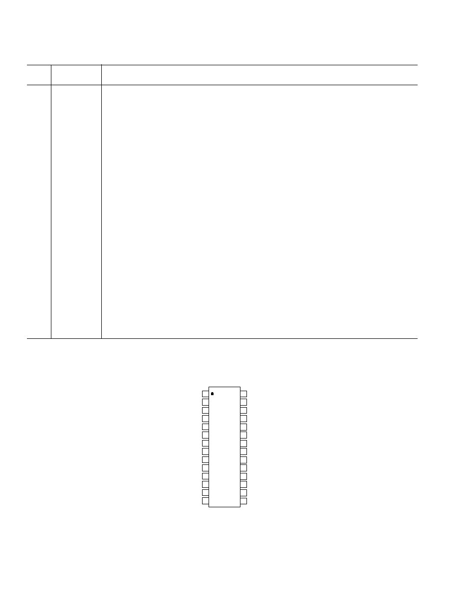
PIN CONFIGURATION
SOIC/SSOP
TOP VIEW
(Not to Scale)
28
27
26
25
24
23
22
21
20
19
18
17
16
15
1
2
3
4
5
6
7
8
9
10
11
12
13
14
AD7899
OPGND
DB7
DB8
DB9
DB10
DB11
DB12
VREF
GND
VINB
VINA
DB13
GND
VDD
VDRIVE
DB6
DB5
DB4
DB3
DB2
DB1
STBY
CLKIN
CONVST
CS
DB0
BUSY/
EOC
RD
相关PDF资料 |
PDF描述 |
|---|---|
| VE-B12-MX-F1 | CONVERTER MOD DC/DC 15V 75W |
| VE-JT2-MY-F4 | CONVERTER MOD DC/DC 15V 50W |
| VE-B12-MW | CONVERTER MOD DC/DC 15V 100W |
| LTC1867LACGN#PBF | IC ADC 16BIT 8CH 175KSPS 16SSOP |
| VE-JT2-MY-F3 | CONVERTER MOD DC/DC 15V 50W |
相关代理商/技术参数 |
参数描述 |
|---|---|
| AD7899ARSZ-2REEL | 功能描述:IC ADC 14BIT 400KSPS 5V 28SSOP RoHS:是 类别:集成电路 (IC) >> 数据采集 - 模数转换器 系列:- 标准包装:1,000 系列:- 位数:12 采样率(每秒):300k 数据接口:并联 转换器数目:1 功率耗散(最大):75mW 电压电源:单电源 工作温度:0°C ~ 70°C 安装类型:表面贴装 封装/外壳:24-SOIC(0.295",7.50mm 宽) 供应商设备封装:24-SOIC 包装:带卷 (TR) 输入数目和类型:1 个单端,单极;1 个单端,双极 |
| AD7899ARSZ-3 | 功能描述:IC ADC 14BIT 400KSPS 5V 28SSOP RoHS:是 类别:集成电路 (IC) >> 数据采集 - 模数转换器 系列:- 标准包装:1,000 系列:- 位数:12 采样率(每秒):300k 数据接口:并联 转换器数目:1 功率耗散(最大):75mW 电压电源:单电源 工作温度:0°C ~ 70°C 安装类型:表面贴装 封装/外壳:24-SOIC(0.295",7.50mm 宽) 供应商设备封装:24-SOIC 包装:带卷 (TR) 输入数目和类型:1 个单端,单极;1 个单端,双极 |
| AD7899ARSZ-3REEL | 功能描述:IC ADC 14BIT 400KSPS 5V 28SSOP RoHS:是 类别:集成电路 (IC) >> 数据采集 - 模数转换器 系列:- 标准包装:1,000 系列:- 位数:12 采样率(每秒):300k 数据接口:并联 转换器数目:1 功率耗散(最大):75mW 电压电源:单电源 工作温度:0°C ~ 70°C 安装类型:表面贴装 封装/外壳:24-SOIC(0.295",7.50mm 宽) 供应商设备封装:24-SOIC 包装:带卷 (TR) 输入数目和类型:1 个单端,单极;1 个单端,双极 |
| AD7899ARZ-1 | 功能描述:IC ADC 14BIT 400KSPS 5V 28SOIC RoHS:是 类别:集成电路 (IC) >> 数据采集 - 模数转换器 系列:- 其它有关文件:TSA1204 View All Specifications 标准包装:1 系列:- 位数:12 采样率(每秒):20M 数据接口:并联 转换器数目:2 功率耗散(最大):155mW 电压电源:模拟和数字 工作温度:-40°C ~ 85°C 安装类型:表面贴装 封装/外壳:48-TQFP 供应商设备封装:48-TQFP(7x7) 包装:Digi-Reel® 输入数目和类型:4 个单端,单极;2 个差分,单极 产品目录页面:1156 (CN2011-ZH PDF) 其它名称:497-5435-6 |
| AD7899ARZ-1REEL | 功能描述:IC ADC 14BIT 400KSPS 5V 28SOIC RoHS:是 类别:集成电路 (IC) >> 数据采集 - 模数转换器 系列:- 标准包装:1,000 系列:- 位数:12 采样率(每秒):300k 数据接口:并联 转换器数目:1 功率耗散(最大):75mW 电压电源:单电源 工作温度:0°C ~ 70°C 安装类型:表面贴装 封装/外壳:24-SOIC(0.295",7.50mm 宽) 供应商设备封装:24-SOIC 包装:带卷 (TR) 输入数目和类型:1 个单端,单极;1 个单端,双极 |
发布紧急采购,3分钟左右您将得到回复。