- 您现在的位置:买卖IC网 > PDF目录10195 > AD7899ARZ-3 (Analog Devices Inc)IC ADC 14BIT 400KSPS 5V 28SOIC PDF资料下载
参数资料
| 型号: | AD7899ARZ-3 |
| 厂商: | Analog Devices Inc |
| 文件页数: | 2/16页 |
| 文件大小: | 0K |
| 描述: | IC ADC 14BIT 400KSPS 5V 28SOIC |
| 标准包装: | 27 |
| 位数: | 14 |
| 采样率(每秒): | 400k |
| 数据接口: | 并联 |
| 转换器数目: | 1 |
| 功率耗散(最大): | 125mW |
| 电压电源: | 单电源 |
| 工作温度: | -40°C ~ 85°C |
| 安装类型: | 表面贴装 |
| 封装/外壳: | 28-SOIC(0.295",7.50mm 宽) |
| 供应商设备封装: | 28-SOIC W |
| 包装: | 管件 |
| 输入数目和类型: | 1 个差分,双极 |
| 配用: | EVAL-AD7899CBZ-ND - BOARD EVAL FOR AD7899 |
REV. A
AD7899
–10–
AD7899-3
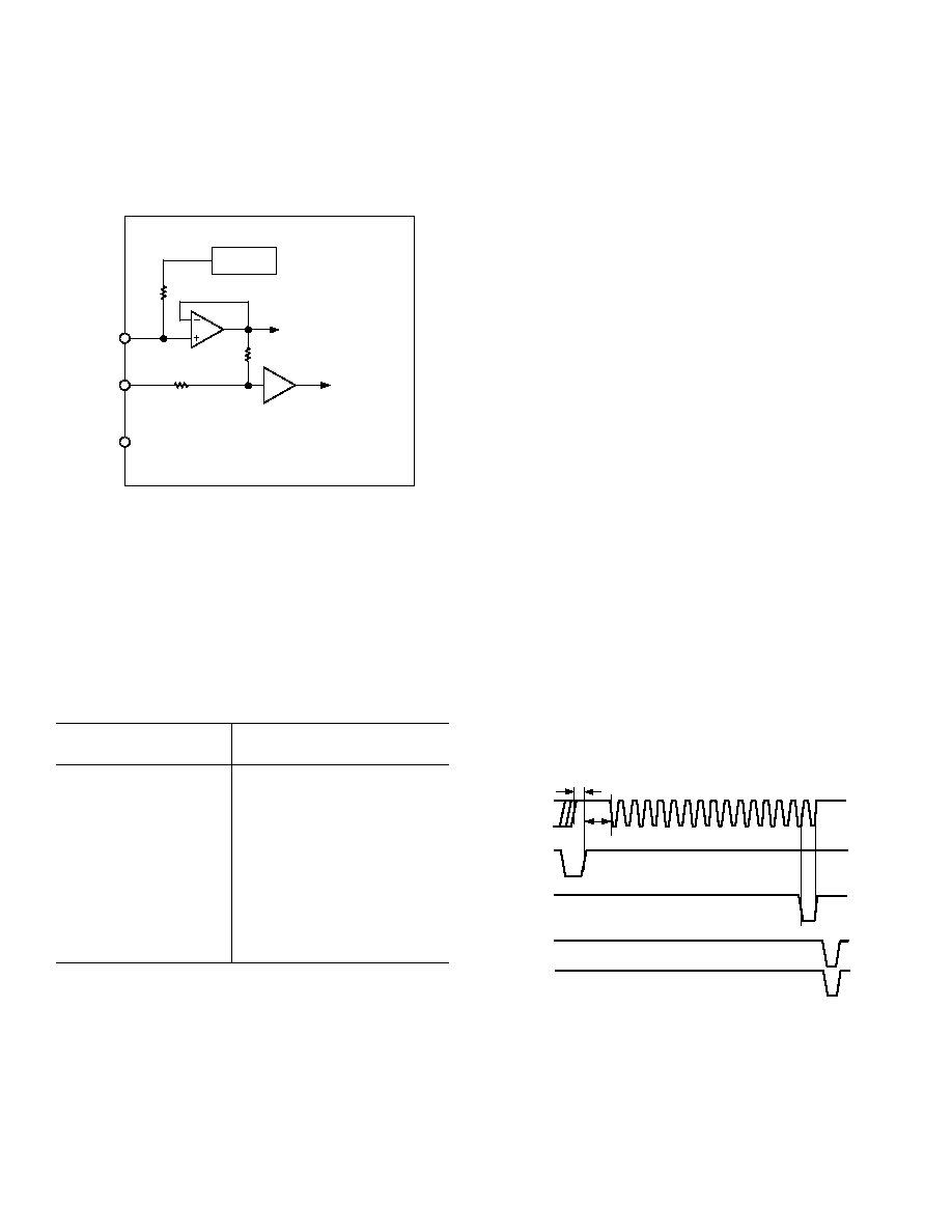
Figure 4 shows the analog input section of the AD7899-3. The
analog input range is
±2.5 V on the VINA input. The VINB input
can be left unconnected but if it is connected to a potential then
that potential must be GND.
AD7899-3
VINA
TRACK/HOLD
TO ADC
REFERENCE
CIRCUITRY
TO INTERNAL
COMPARATOR
R1
R2
6k
2.5V
REFERENCE
VINB
VREF
Figure 4. AD7899-3 Analog Input Structure
For the AD7899-3, R1 = 4 k
and R2 = 4 k. The resistor
input stage is followed by the high input impedance stage of the
track/hold amplifier.
The designed code transitions take place midway between suc-
cessive integer LSB values (i.e., 1/2 LSB, 3/2 LSBs, 5/2 LSBs
etc.) LSB size is given by the formula, 1 LSB = FSR/16384.
Output coding is two’s complement binary with 1 LSB = FSR/
16384 = 5 V/16384 = 610.4
V. The ideal input/output transfer
function for the AD7899-3 is shown in Table III.
Table III. Ideal Input/Output Code Table for the AD7899-3
Digital Output
Analog Input
l
Code Transition
+FSR/2 – 3/2 LSB
2
011 . . . 110 to 011 . . . 111
+FSR/2 – 5/2 LSB
011 . . . 101 to 011 . . . 110
+FSR/2 – 7/2 LSB
011 . . . 100 to 011 . . . 101
GND + 3/2 LSB
000 . . . 001 to 000 . . . 010
GND + 1/2 LSB
000 . . . 000 to 000 . . . 001
GND – 1/2 LSB
111 . . . 111 to 000 . . . 000
GND – 3/2 LSB
111 . . . 110 to 111 . . . 111
–FSR/2 + 5/2 LSB
100 . . . 010 to 100 . . . 011
–FSR/2 + 3/2 LSB
100 . . . 001 to 100 . . . 010
–FSR/2 + 1/2 LSB
100 . . . 000 to 100 . . . 001
NOTES
1FSR is full-scale range is 5 V, with V
REF = 2.5 V
21 LSB = FSR/16384 = 610.4
V (±2.5 V – AD7899-3) with V
REF = 2.5 V.
TIMING AND CONTROL
Starting a Conversion
The conversion is initiated by applying a rising edge to the
CONVST signal. This places the track/hold into hold mode and
starts the conversion. The status of the conversion is indicated
by the dual function signal BUSY/
EOC. The AD7899 can operate
in two conversion modes,
EOC (End Of Conversion) mode and
BUSY mode. The operating mode is determined by the state of
CONVST at the end of the conversion.
Selecting a Conversion Clock
The AD7899 has an internal laser trimmed oscillator which can
be used to control the conversion process. Alternatively an external
clock source can be used to control the conversion process. The
highest external clock frequency allowed is 6.5 MHz. This means
a conversion time of 2.46
s compared to 2.2 s using the inter-
nal clock. However in some instances it may be useful to use an
external clock when high throughput rates are not required. For
example two or more AD7899s may be synchronized by using
the same external clock for all devices. In this way there is no
latency between output logic signals due to differences in the
frequency of the internal clock oscillators.
On the rising edge of
CONVST the AD7899 will examine the
status of the CLKIN pin. If this pin is low it will use the internal
laser trimmed oscillator as the conversion clock. If the CLKIN pin
is high the AD7899 will wait for an external clock to be supplied
to this pin which will then be used as the conversion clock. The
first falling edge of the external clock should not happen for at
least 100 ns after the rising edge of
CONVST to ensure correct
operation. Figure 5 shows how the BUSY/
EOC output is synchro-
nized to the CLKIN signal. Each conversion requires 16 clocks.
The result of the conversion is transferred to the output data
register on the falling edge of the 15th clock cycle. When the
internal clock is selected the status of the CLKIN pin is free to
change during conversion but the CLKIN setup and hold times
must be observed in order to ensure that the correct conversion
clock is used. The CLKIN pin can also be tied low permanently if
the internal conversion clock is to be used.
CONVST
BUSY/
EOC
RD
CS
CLKIN
1 2 3 4 5 6
7 8 9 10 11 1213 14 1516
t9
t11
Figure 5. Using an External Clock
相关PDF资料 |
PDF描述 |
|---|---|
| A6FBXAU | CONN PLUG CORD FMAL 6PIN BLK/AU |
| VE-23M-MX-F1 | CONVERTER MOD DC/DC 10V 75W |
| VI-2W1-MY | CONVERTER MOD DC/DC 12V 50W |
| MS3114P14-5P | CONN RCPT 5POS JAM NUT W/PINS |
| CXC3106A14S-2S-300 | CONN PLUG 4POS STRGHT SKT |
相关代理商/技术参数 |
参数描述 |
|---|---|
| AD7899BR-1 | 功能描述:IC ADC 14BIT 400KSPS 5V 28-SOIC RoHS:否 类别:集成电路 (IC) >> 数据采集 - 模数转换器 系列:- 标准包装:1 系列:- 位数:14 采样率(每秒):83k 数据接口:串行,并联 转换器数目:1 功率耗散(最大):95mW 电压电源:双 ± 工作温度:0°C ~ 70°C 安装类型:通孔 封装/外壳:28-DIP(0.600",15.24mm) 供应商设备封装:28-PDIP 包装:管件 输入数目和类型:1 个单端,双极 |
| AD7899BR-1REEL | 制造商:Analog Devices 功能描述:ADC SGL SAR 400KSPS 14BIT PARALLEL 28SOIC W - Tape and Reel |
| AD7899BR-1REEL7 | 功能描述:IC ADC 14BIT 400KSPS 5V 28-SOIC RoHS:否 类别:集成电路 (IC) >> 数据采集 - 模数转换器 系列:- 产品培训模块:Lead (SnPb) Finish for COTS Obsolescence Mitigation Program 标准包装:2,500 系列:- 位数:12 采样率(每秒):3M 数据接口:- 转换器数目:- 功率耗散(最大):- 电压电源:- 工作温度:- 安装类型:表面贴装 封装/外壳:SOT-23-6 供应商设备封装:SOT-23-6 包装:带卷 (TR) 输入数目和类型:- |
| AD7899BR-3 | 制造商:Rochester Electronics LLC 功能描述:14-BIT BIPOLAR INPUT SINGLE SUPPLY ADC - Bulk 制造商:Analog Devices 功能描述: |
| AD7899BR-3REEL | 制造商:Analog Devices 功能描述:ADC SGL SAR 400KSPS 14BIT PARALLEL 28SOIC W - Tape and Reel |
发布紧急采购,3分钟左右您将得到回复。