- 您现在的位置:买卖IC网 > PDF目录10147 > AD7899BR-1 (Analog Devices Inc)IC ADC 14BIT 400KSPS 5V 28-SOIC PDF资料下载
参数资料
| 型号: | AD7899BR-1 |
| 厂商: | Analog Devices Inc |
| 文件页数: | 3/16页 |
| 文件大小: | 0K |
| 描述: | IC ADC 14BIT 400KSPS 5V 28-SOIC |
| 标准包装: | 27 |
| 位数: | 14 |
| 采样率(每秒): | 400k |
| 数据接口: | 并联 |
| 转换器数目: | 1 |
| 功率耗散(最大): | 125mW |
| 电压电源: | 单电源 |
| 工作温度: | -40°C ~ 85°C |
| 安装类型: | 表面贴装 |
| 封装/外壳: | 28-SOIC(0.295",7.50mm 宽) |
| 供应商设备封装: | 28-SOIC W |
| 包装: | 管件 |
| 输入数目和类型: | 1 个差分,双极 |
| 配用: | EVAL-AD7899CBZ-ND - BOARD EVAL FOR AD7899 |
REV. A
AD7899
–11–
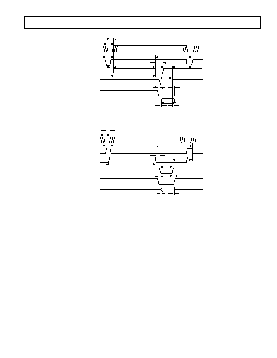
EOC Mode
The
CONVST signal is normally high. Pulsing the CONVST low
will initiate a conversion on its rising edge. The state of the
CONVST signal is checked at the end of conversion. Since the
CONVST will be high when this happens the AD7899 BUSY/
EOC pin will take on its EOC function and bring the BUSY/EOC
line low for one clock period before returning high again. In this
mode the
EOC can be tied to the RD and CS signals to allow
automatic reading of the conversion result if required. The timing
diagram for operation in
EOC mode is shown in Figure 6.
BUSY Mode
The
CONVST signal is normally low. Pulsing the CONVST
high will initiate a conversion on its rising edge. The state of the
CONVST signal is checked at the end of conversion. Since the
CONVST will be low when this happens the AD7899 BUSY/
EOC pin will take on its BUSY function will bring BUSY/EOC
low, indicating that the conversion is complete. BUSY/
EOC will
remain low until the next rising edge of
CONVST where BUSY/
EOC returns high. The timing diagram for operation in BUSY
mode is shown in Figure 7.
Continuous Conversion Mode
When the AD7899 is used with an external clock, connecting
the CLKIN and
CONVST signals together will cause the AD7899
to continuously perform conversions. As each conversion com-
pletes the BUSY/
EOC pin will pulse low for one clock period
(
EOC function) indicating that the conversion result is available.
Figure 8 shows the timing and control sequence of the AD7899
in Continuous Conversion Mode.
Reading Data from the AD7899
Data is read from the part via a 14-bit parallel data bus with
standard
CS and RD signals. The CS and RD inputs are inter-
nally gated to enable the conversion result onto the data bus.
The data lines DB0 to DB13 leave their high impedance state
when both
CS and RD are logic low. Therefore CS may be
permanently tied logic low and the
RD signal used to access the
conversion result if required. Figures 6 and 7 show a timing
specification called “Quiet Time.” This is the amount of time
which should be left after a read operation and before the next
conversion is initiated. The quiet time depends heavily on data
bus capacitance but a figure of 50 ns to 100 ns is typical, with a
worst case figure of 150 ns.
t8
tEOC
t2
t1
t9
DATA
CONVST
BUSY/
EOC
RD
CS
QUIET
TIME
THREE-STATE
CLKIN
THREE-STATE
t3
t10
t4
t6
t7
tCONV
tACQ
t5
Figure 6. Conversion Sequence Timing Diagram (EOC Mode)
t8
t1
DATA
CONVST
BUSY/
EOC
RD
CS
CLKIN
THREE-STATE
QUIET
TIME
t10
t3
t6
tACQ
t5
t9
t4
t7
tCONV
Figure 7. Conversion Sequence Timing Diagram (BUSY Mode)
相关PDF资料 |
PDF描述 |
|---|---|
| MS27468T9F35PA | CONN RCPT 6POS JAM NUT W/PINS |
| VE-242-IU-F2 | CONVERTER MOD DC/DC 15V 200W |
| VE-B3Y-IV-B1 | CONVERTER MOD DC/DC 3.3V 99W |
| VE-241-IU-F4 | CONVERTER MOD DC/DC 12V 200W |
| MS3106F20-29SZ | CONN PLUG 17POS STRAIGHT W/SCKT |
相关代理商/技术参数 |
参数描述 |
|---|---|
| AD7899BR-1REEL | 制造商:Analog Devices 功能描述:ADC SGL SAR 400KSPS 14BIT PARALLEL 28SOIC W - Tape and Reel |
| AD7899BR-1REEL7 | 功能描述:IC ADC 14BIT 400KSPS 5V 28-SOIC RoHS:否 类别:集成电路 (IC) >> 数据采集 - 模数转换器 系列:- 产品培训模块:Lead (SnPb) Finish for COTS Obsolescence Mitigation Program 标准包装:2,500 系列:- 位数:12 采样率(每秒):3M 数据接口:- 转换器数目:- 功率耗散(最大):- 电压电源:- 工作温度:- 安装类型:表面贴装 封装/外壳:SOT-23-6 供应商设备封装:SOT-23-6 包装:带卷 (TR) 输入数目和类型:- |
| AD7899BR-3 | 制造商:Rochester Electronics LLC 功能描述:14-BIT BIPOLAR INPUT SINGLE SUPPLY ADC - Bulk 制造商:Analog Devices 功能描述: |
| AD7899BR-3REEL | 制造商:Analog Devices 功能描述:ADC SGL SAR 400KSPS 14BIT PARALLEL 28SOIC W - Tape and Reel |
| AD7899BR-3REEL7 | 制造商:Analog Devices 功能描述: 制造商:Rochester Electronics LLC 功能描述: |
发布紧急采购,3分钟左右您将得到回复。