- 您现在的位置:买卖IC网 > PDF目录10533 > AD7899BRZ-1 (Analog Devices Inc)IC ADC 14BIT 400KSPS 5V 28SOIC PDF资料下载
参数资料
| 型号: | AD7899BRZ-1 |
| 厂商: | Analog Devices Inc |
| 文件页数: | 11/16页 |
| 文件大小: | 0K |
| 描述: | IC ADC 14BIT 400KSPS 5V 28SOIC |
| 标准包装: | 27 |
| 位数: | 14 |
| 采样率(每秒): | 400k |
| 数据接口: | 并联 |
| 转换器数目: | 1 |
| 功率耗散(最大): | 125mW |
| 电压电源: | 单电源 |
| 工作温度: | -40°C ~ 85°C |
| 安装类型: | 表面贴装 |
| 封装/外壳: | 28-SOIC(0.295",7.50mm 宽) |
| 供应商设备封装: | 28-SOIC W |
| 包装: | 管件 |
| 输入数目和类型: | 1 个差分,双极 |
| 配用: | EVAL-AD7899CBZ-ND - BOARD EVAL FOR AD7899 |
REV. A
AD7899
–4–
TIMING CHARACTERISTICS1, 2
A, B and S
Parameter
Versions
Unit
Test Conditions/Comments
tCONV
2.2
s max
Conversion Time, Internal Clock
2.46
s max
CLKIN = 6.5 MHz
tACQ
0.3
s max
Acquisition Time
tEOC
120
ns min
EOC Pulsewidth
180
ns max
tWAKE-UP – External VREF
5
2
s max
STBY Rising Edge to CONVST Rising Edge
(See Standby Mode Operation)
t1
35
ns min
CONVST Pulsewidth
t2
70
ns min
CONVST Rising Edge to BUSY Rising Edge
Read Operation
t3
0
ns min
CS to RD Setup Time
t4
0
ns min
CS to RD Hold Time
t5
35
ns min
Read Pulsewidth
t6
3
35
ns max
Data Access Time after Falling Edge of
RD, V
DRIVE = 5 V
40
ns max
Data Access Time after Falling Edge of
RD, V
DRIVE = 3 V
t7
4
5
ns min
Bus Relinquish Time after Rising Edge of
RD
30
ns max
t8
0
ns min
BUSY Falling Edge to
RD Delay
External Clock
t9
0
ns min
CLKIN to
CONVST Rising Edge Setup Time
t10
20
ns min
CLKIN to
CONVST Rising Edge Hold Time
t11
100
ns min
CONVST Rising Edge to CLK Falling Edge
NOTES
1 Sample tested at 25
°C to ensure compliance. All input signals are measured with tr = tf = 1 ns (10% to 90% of V
DRIVE) and timed from a voltage level of V DRIVE/2.
2 See Figures 5, 6, 7, and 8.
3 Measured with the load circuit of Figure 1 and defined as the time required for an output to cross 0.8 V or 2.0 V.
4These times are derived from the measured time taken by the data outputs to change 0.5 V when loaded with the circuit of Figure 1. The measured number is then
extrapolated back to remove the effects of charging or discharging the 50 pF capacitor. This means that the times quoted in the timing characteristics are the true bus
relinquish times of the part and as such are independent of external bus loading capacitances.
5 Refer to the Standby Mode Operation section.
Specifications subject to change without notice.
(VDD = 5 V
5%, AGND = DGND = 0 V, VREF = Internal, Clock = Internal; All specifications TMIN
to TMAX and valid for VDRIVE = 3 V
5% and 5 V
5% unless otherwise noted.)
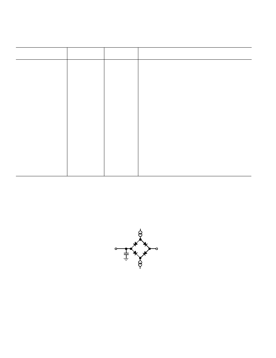
1.6mA
1.6V
400 A
50pF
TO
OUTPUT
PIN
Figure 1. Load Circuit for Access Time and Bus Relinquish Time
相关PDF资料 |
PDF描述 |
|---|---|
| MS3106A12S-3S | CONN PLUG 2POS STRAIGHT W/SCKT |
| AD9649BCPZ-20 | IC ADC 14BIT 20MSPS 32LFCSP |
| 97-3101A-14S-6S | CONN RECEPT CBL MNT 6POS W/SOCK |
| VE-J3V-MY-F1 | CONVERTER MOD DC/DC 5.8V 50W |
| LTC1741CFW | IC ADC 12BIT 65MSPS 48-TSSOP |
相关代理商/技术参数 |
参数描述 |
|---|---|
| AD7899BRZ-3 | 功能描述:IC ADC 14BIT 400KSPS 5V 28SOIC RoHS:是 类别:集成电路 (IC) >> 数据采集 - 模数转换器 系列:- 标准包装:1,000 系列:- 位数:12 采样率(每秒):300k 数据接口:并联 转换器数目:1 功率耗散(最大):75mW 电压电源:单电源 工作温度:0°C ~ 70°C 安装类型:表面贴装 封装/外壳:24-SOIC(0.295",7.50mm 宽) 供应商设备封装:24-SOIC 包装:带卷 (TR) 输入数目和类型:1 个单端,单极;1 个单端,双极 |
| AD7899SR-1 | 功能描述:模数转换器 - ADC 5V SGL Supply 14-Bit 400 kSPS RoHS:否 制造商:Analog Devices 通道数量: 结构: 转换速率: 分辨率: 输入类型: 信噪比: 接口类型: 工作电源电压: 最大工作温度: 安装风格: 封装 / 箱体: |
| AD7899SR-1REEL | 制造商:Analog Devices 功能描述:ADC SGL SAR 400KSPS 14BIT PARALLEL 28SOIC W - Tape and Reel |
| AD7899SR-1REEL7 | 功能描述:模数转换器 - ADC 5V SGL Supply 14-Bit 400 kSPS RoHS:否 制造商:Analog Devices 通道数量: 结构: 转换速率: 分辨率: 输入类型: 信噪比: 接口类型: 工作电源电压: 最大工作温度: 安装风格: 封装 / 箱体: |
| AD7899SRZ-1 | 功能描述:模数转换器 - ADC 5V SGL Supply 14-Bit 400 kSPS RoHS:否 制造商:Analog Devices 通道数量: 结构: 转换速率: 分辨率: 输入类型: 信噪比: 接口类型: 工作电源电压: 最大工作温度: 安装风格: 封装 / 箱体: |
发布紧急采购,3分钟左右您将得到回复。