- 您现在的位置:买卖IC网 > PDF目录10537 > AD7938BSUZ (Analog Devices Inc)IC ADC 12BIT 8CHAN 32TQFP PDF资料下载
参数资料
| 型号: | AD7938BSUZ |
| 厂商: | Analog Devices Inc |
| 文件页数: | 11/36页 |
| 文件大小: | 0K |
| 描述: | IC ADC 12BIT 8CHAN 32TQFP |
| 标准包装: | 1 |
| 位数: | 12 |
| 采样率(每秒): | 1.5M |
| 数据接口: | 并联 |
| 转换器数目: | 1 |
| 功率耗散(最大): | 13.5mW |
| 电压电源: | 单电源 |
| 工作温度: | -40°C ~ 85°C |
| 安装类型: | 表面贴装 |
| 封装/外壳: | 32-TQFP |
| 供应商设备封装: | 32-TQFP(7x7) |
| 包装: | 托盘 |
| 输入数目和类型: | 8 个单端,单极;4 个差分,单极;4 个伪差分,单极;7 伪差分,单极 |
| 配用: | EVAL-AD7938CBZ-ND - EVAL BOARD FOR AD7938 |
第1页第2页第3页第4页第5页第6页第7页第8页第9页第10页当前第11页第12页第13页第14页第15页第16页第17页第18页第19页第20页第21页第22页第23页第24页第25页第26页第27页第28页第29页第30页第31页第32页第33页第34页第35页第36页
Data Sheet
AD7938/AD7939
Rev. C | Page 19 of 36
03
71
5-
02
6
100...000
011...111
1LSB = 2× VREF/4096 (AD7938)
1LSB = 2× VREF/1024 (AD7939)
–VREF +1 LSB
VREF
+VREF –1 LSB
ADC
CO
DE
100...001
100...010
011...110
000...001
000...000
111...111
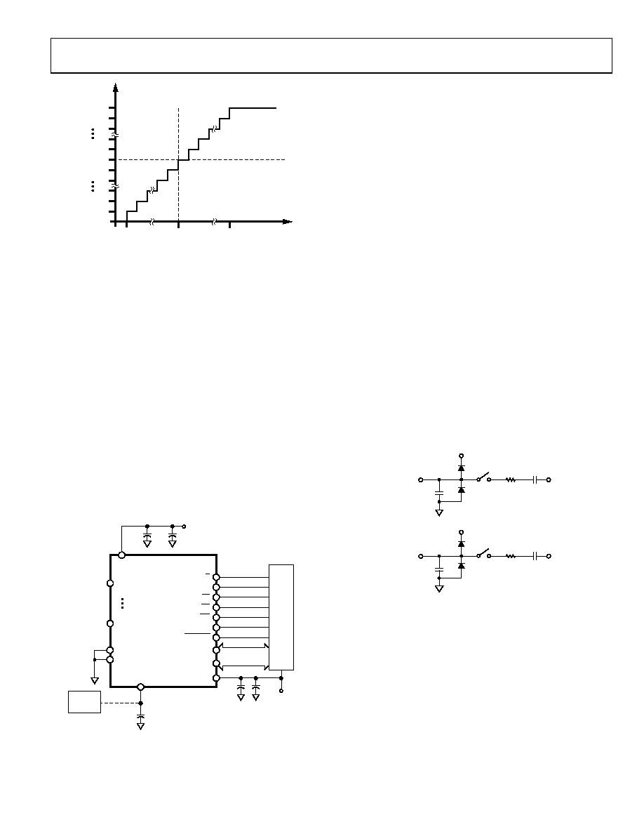
Figure 18. AD7938/AD7939 Ideal Transfer Characteristic
with Twos Complement Output Coding and 2 × VREF Range
TYPICAL CONNECTION DIAGRAM
Figure 19 shows a typical connection diagram for the
AD7938/AD7939. The AGND and DGND pins are connected
together at the device for good noise suppression. The
VREFIN/VREFOUT pin is decoupled to AGND with a 0.47 μF
capacitor to avoid noise pickup if the internal reference is used.
Alternatively, VREFIN/VREFOUT can be connected to an external
reference source. In this case, the reference pin should be
decoupled with a 0.1 μF capacitor. In both cases, the analog
input range can either be 0 V to VREF (RANGE bit = 0) or 0 V to
2 × VREF (RANGE bit = 1). The analog input configuration can
be either eight single-ended inputs, four differential pairs, four
pseudo differential pairs, or seven pseudo differential inputs
supply. The voltage applied to the VDRIVE input controls the
voltage of the digital interface. Here, it is connected to the same
3 V supply of the microprocessor to allow a 3 V logic interface
(see the Digital Inputs section).
0.1F
10F
3V/5V
SUPPLY
3V
SUPPLY
AD7938/AD7939
0.1F
0.1F EXTERNAL VREF
0.47F INTERNAL VREF
AGND
DGND
W/B
CLKIN
CS
VDRIVE
VDD
VREFIN/VREFOUT
10F
2.5V
VREF
RD
CONVST
WR
BUSY
DB0
DB11/DB9
03
71
5-
02
7
+
0 TO VREF/
0 TO 2 × VREF
VIN0
VIN7
M
ICRO
CO
NT
RO
L
E
R/
M
ICR
O
P
RO
CE
S
O
R
Figure 19. Typical Connection Diagram
ANALOG INPUT STRUCTURE
Figure 20 shows the equivalent circuit of the analog input
structure of the AD7938/AD7939 in differential/pseudo
differential mode. In single-ended mode, VIN is internally
tied to AGND. The four diodes provide ESD protection for the
analog inputs. Care must be taken to ensure that the analog
input signals never exceed the supply rails by more than
300 mV. Doing so causes these diodes to become forward-
biased and start conducting into the substrate. These diodes can
conduct up to 10 mA without causing irreversible damage to
the part.
The C1 capacitors in Figure 20 are typically 4 pF and can
primarily be attributed to pin capacitance. The resistors are
lumped components made up of the on resistance of the
switches. The value of these resistors is typically about 100 Ω.
The C2 capacitors are the sampling capacitors of the ADC and
typically have a capacitance of 45 pF.
For ac applications, removing high frequency components from
the analog input signal is recommended by the use of an RC
low-pass filter on the relevant analog input pins. In applications
where harmonic distortion and signal-to-noise ratio are critical,
the analog input should be driven from a low impedance
source. Large source impedances significantly affect the ac
performance of the ADC. This may necessitate the use of an
input buffer amplifier. The choice of the op amp is a function of
the particular application.
R1
C2
VIN+
VDD
C1
D
0
371
5-
0
28
R1
C2
VIN–
VDD
C1
D
Figure 20. Equivalent Analog Input Circuit,
Conversion Phase: Switches Open, Track Phase: Switches Closed
When no amplifier is used to drive the analog input, the source
impedance should be limited to low values. The maximum
source impedance depends on the amount of THD that can be
tolerated. The THD increases as the source impedance increases
and performance degrades. Figure 21 and Figure 22 show a
graph of the THD vs. source impedance with a 50 kHz input
tone for both VDD = 5 V and 3 V in single-ended mode and fully
differential mode, respectively.
相关PDF资料 |
PDF描述 |
|---|---|
| VI-B41-MW | CONVERTER MOD DC/DC 12V 100W |
| AD7650ASTZ | IC ADC 16BIT 570KSPS 48LQFP |
| AD7694BRMZ | IC ADC 16BIT SRL 250KSPS 8MSOP |
| VI-2TR-MX | CONVERTER MOD DC/DC 7.5V 75W |
| ISL3152EIUZ-T7A | IC LINEAR |
相关代理商/技术参数 |
参数描述 |
|---|---|
| AD7938BSUZ6 | 制造商:AD 功能描述:Pb Free |
| AD7938BSUZ-6 | 功能描述:IC ADC 12BIT 8CHAN 32TQFP RoHS:是 类别:集成电路 (IC) >> 数据采集 - 模数转换器 系列:- 标准包装:1,000 系列:- 位数:16 采样率(每秒):45k 数据接口:串行 转换器数目:2 功率耗散(最大):315mW 电压电源:模拟和数字 工作温度:0°C ~ 70°C 安装类型:表面贴装 封装/外壳:28-SOIC(0.295",7.50mm 宽) 供应商设备封装:28-SOIC W 包装:带卷 (TR) 输入数目和类型:2 个单端,单极 |
| AD7938BSUZ-6REEL7 | 功能描述:IC ADC 12BIT 8CHAN 32TQFP RoHS:是 类别:集成电路 (IC) >> 数据采集 - 模数转换器 系列:- 其它有关文件:TSA1204 View All Specifications 标准包装:1 系列:- 位数:12 采样率(每秒):20M 数据接口:并联 转换器数目:2 功率耗散(最大):155mW 电压电源:模拟和数字 工作温度:-40°C ~ 85°C 安装类型:表面贴装 封装/外壳:48-TQFP 供应商设备封装:48-TQFP(7x7) 包装:Digi-Reel® 输入数目和类型:4 个单端,单极;2 个差分,单极 产品目录页面:1156 (CN2011-ZH PDF) 其它名称:497-5435-6 |
| AD7938BSUZ-REEL7 | 功能描述:IC ADC 12BIT 8CHAN 32TQFP RoHS:是 类别:集成电路 (IC) >> 数据采集 - 模数转换器 系列:- 标准包装:1,000 系列:- 位数:12 采样率(每秒):300k 数据接口:并联 转换器数目:1 功率耗散(最大):75mW 电压电源:单电源 工作温度:0°C ~ 70°C 安装类型:表面贴装 封装/外壳:24-SOIC(0.295",7.50mm 宽) 供应商设备封装:24-SOIC 包装:带卷 (TR) 输入数目和类型:1 个单端,单极;1 个单端,双极 |
| AD7939 | 制造商:AD 制造商全称:Analog Devices 功能描述:8-Channel, 1.5 MSPS, 12-Bit and 10-Bit Parallel ADCs with a Sequencer |
发布紧急采购,3分钟左右您将得到回复。