- 您现在的位置:买卖IC网 > PDF目录10544 > AD7939BSUZ (Analog Devices Inc)IC ADC 10BIT 8CH PARALL 32TQFP PDF资料下载
参数资料
| 型号: | AD7939BSUZ |
| 厂商: | Analog Devices Inc |
| 文件页数: | 14/36页 |
| 文件大小: | 0K |
| 描述: | IC ADC 10BIT 8CH PARALL 32TQFP |
| 标准包装: | 1 |
| 位数: | 10 |
| 采样率(每秒): | 1.5M |
| 数据接口: | 并联 |
| 转换器数目: | 1 |
| 功率耗散(最大): | 13.5mW |
| 电压电源: | 单电源 |
| 工作温度: | -40°C ~ 85°C |
| 安装类型: | 表面贴装 |
| 封装/外壳: | 32-TQFP |
| 供应商设备封装: | 32-TQFP(7x7) |
| 包装: | 托盘 |
| 输入数目和类型: | 8 个单端,单极;4 个差分,单极;4 个伪差分,单极;7 伪差分,单极 |
| 配用: | EVAL-AD7939CBZ-ND - BOARD EVALUATION FOR AD7939CBZ |
第1页第2页第3页第4页第5页第6页第7页第8页第9页第10页第11页第12页第13页当前第14页第15页第16页第17页第18页第19页第20页第21页第22页第23页第24页第25页第26页第27页第28页第29页第30页第31页第32页第33页第34页第35页第36页
Data Sheet
AD7938/AD7939
Rev. C | Page 21 of 36
03715-
032
VREF
p-p
VIN+
VIN–
VREF
p-p
*ADDITIONAL PINS OMITTED FOR CLARITY.
AD7938/
AD7939*
COMMON-MODE
VOLTAGE
Figure 25. Differential Input Definition
The amplitude of the differential signal is the difference
between the signals applied to the VIN+ and VIN pins in each
differential pair (that is, VIN+ VIN). VIN+ and VIN should be
simultaneously driven by two signals each of amplitude VREF (or
2 × VREF depending on the range chosen) that are 180° out of
phase. The amplitude of the differential signal is therefore VREF
to +VREF peak-to-peak (that is, 2 × VREF). This is regardless of
the common mode (CM). The common mode is the average of
the two signals (that is, (VIN+ + VIN)/2) and is therefore the
voltage on which the two inputs are centered. This results in the
span of each input being CM ± VREF/2. This voltage has to be set
up externally and its range varies with the reference value VREF.
As the value of VREF increases, the common-mode range
decreases. When driving the inputs with an amplifier, the actual
common-mode range is determined by the amplifier’s output
voltage swing.
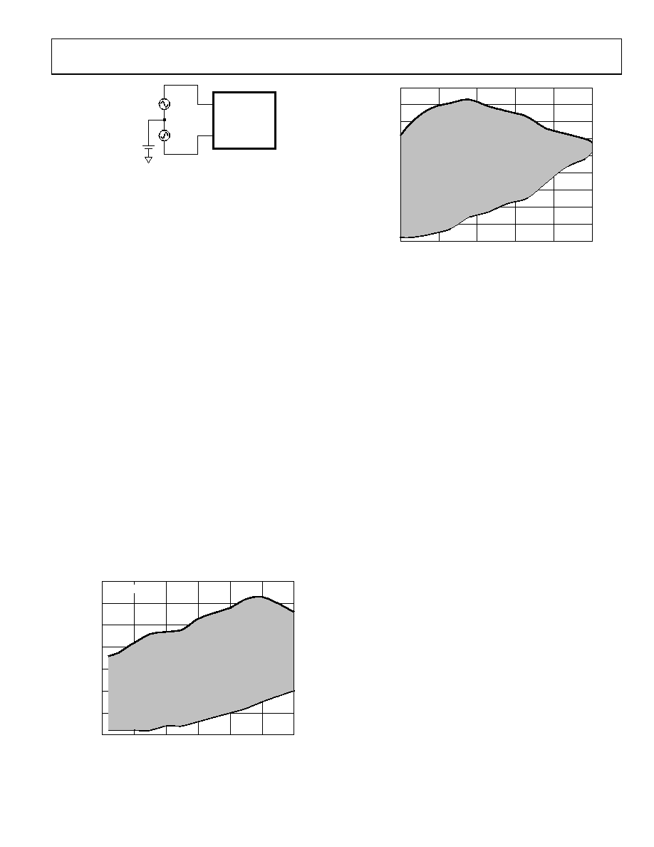
Figure 26 and Figure 27 show how the common-mode range
typically varies with VREF for a 5 V power supply using the 0 V
to VREF range or 2 × VREF range, respectively. The common
mode must be in this range to guarantee the functionality of
the AD7938/AD7939.
When a conversion takes place, the common mode is rejected,
resulting in a virtually noise-free signal of amplitude VREF to
+VREF, corresponding to the digital codes of 0 to 4096 for the
AD7938 and 0 to 1024 for the AD7939. If the 2 × VREF range is
used, the input signal amplitude extends from 2 VREF to +2 VREF
after conversion.
VREF (V)
C
O
MMO
N
-MO
D
E
R
A
N
G
E
(V)
3.5
3.0
2.0
1.5
2.5
1.0
0.5
0
0.5
1.5
1.0
2.0
2.5
3.0
03715-
033
TA = 25°C
Figure 26. Input Common-Mode Range vs. VREF (0 V to VREF Range, VDD = 5 V)
VREF (V)
C
O
MMO
N
-MO
D
E
R
A
N
G
E
(V)
4.5
4.0
3.0
1.5
2.0
2.5
3.5
1.0
0.5
0
0.1
0.6
1.6
1.1
2.1
2.6
03715-
034
TA = 25°C
Figure 27. Input Common-Mode Range vs. VREF (2 × VREF Range, VDD = 5 V)
Driving Differential Inputs
Differential operation requires that VIN+ and VIN be
simultaneously driven with two equal signals that are 180° out
of phase. The common mode must be set up externally and has
a range that is determined by VREF, the power supply, and the
particular amplifier used to drive the analog inputs. Differential
modes of operation with either an ac or dc input provide the
best THD performance over a wide frequency range. Since not
all applications have a signal preconditioned for differential
operation, there is often a need to perform single-ended-to-
differential conversion.
Using an Op Amp Pair
An op amp pair can be used to directly couple a differential
signal to one of the analog input pairs of the AD7938/AD7939.
The circuit configurations shown in Figure 28 and Figure 29
show how a dual op amp can be used to convert a single-ended
signal into a differential signal for both a bipolar and unipolar
input signal, respectively.
The voltage applied to Point A sets up the common-mode
voltage. In both diagrams, it is connected in some way to the
reference, but any value in the common-mode range can be
input here to set up the common mode. A suitable dual op amp
that can be used in this configuration to provide differential
drive to the AD7938/AD7939 is the AD8022.
Take care when choosing the op amp; the selection depends on
the required power supply and system performance objectives.
The driver circuits in Figure 28 and Figure 29 are optimized for
dc coupling applications requiring best distortion performance.
The differential op amp driver circuit in Figure 28 is configured
to convert and level shift a single-ended, ground-referenced
(bipolar) signal to a differential signal centered at the VREF level
of the ADC.
The circuit configuration shown in Figure 29 converts a
unipolar, single-ended signal into a differential signal.
相关PDF资料 |
PDF描述 |
|---|---|
| AD7822BRZ | IC ADC 8BIT 1CH 2MSPS 20-SOIC |
| VE-J43-MW-F2 | CONVERTER MOD DC/DC 24V 100W |
| AD7811YNZ | IC ADC 10BIT 4CHAN SRL 16DIP |
| VI-2TJ-IW-F3 | CONVERTER MOD DC/DC 36V 100W |
| VE-J42-MW-F4 | CONVERTER MOD DC/DC 15V 100W |
相关代理商/技术参数 |
参数描述 |
|---|---|
| AD7939BSUZ-REEL7 | 功能描述:IC ADC 10BIT 8CH PARALL 32TQFP RoHS:是 类别:集成电路 (IC) >> 数据采集 - 模数转换器 系列:- 标准包装:1,000 系列:- 位数:16 采样率(每秒):45k 数据接口:串行 转换器数目:2 功率耗散(最大):315mW 电压电源:模拟和数字 工作温度:0°C ~ 70°C 安装类型:表面贴装 封装/外壳:28-SOIC(0.295",7.50mm 宽) 供应商设备封装:28-SOIC W 包装:带卷 (TR) 输入数目和类型:2 个单端,单极 |
| AD7940 | 制造商:AD 制造商全称:Analog Devices 功能描述:3mW, 100kSPS, 14-Bit ADC in 6-Lead SOT-23 |
| AD7940BRJ | 制造商:Analog Devices 功能描述:100 KSPS, 14_BIT ADC SOT 23 PKG I.C. - Bulk |
| AD7940BRJ-R2 | 制造商:Analog Devices 功能描述:ADC Single SAR 100ksps 14-bit Serial 6-Pin SOT-23 T/R 制造商:Analog Devices 功能描述:ADC SGL SAR 100KSPS 14BIT SERL 6PIN SOT-23 - Tape and Reel |
| AD7940BRJ-REEL7 | 制造商:Rochester Electronics LLC 功能描述: 制造商:Analog Devices 功能描述: |
发布紧急采购,3分钟左右您将得到回复。