参数资料
| 型号: | AD7940BRM |
| 厂商: | Analog Devices Inc |
| 文件页数: | 3/20页 |
| 文件大小: | 0K |
| 描述: | IC ADC 14BIT UNIPOLAR 8-MSOP |
| 标准包装: | 50 |
| 位数: | 14 |
| 采样率(每秒): | 100k |
| 数据接口: | DSP,MICROWIRE?,QSPI?,串行,SPI? |
| 转换器数目: | 1 |
| 功率耗散(最大): | 26.4mW |
| 电压电源: | 单电源 |
| 工作温度: | -40°C ~ 85°C |
| 安装类型: | 表面贴装 |
| 封装/外壳: | 8-TSSOP,8-MSOP(0.118",3.00mm 宽) |
| 供应商设备封装: | 8-MSOP |
| 包装: | 管件 |
| 输入数目和类型: | 1 个单端,单极 |
| 配用: | EVAL-AD7940CBZ-ND - BOARD EVALUATION AD7940 AD7940-DBRD-ND - BOARD EVAL FOR AD7940 STAMP SPI |
AD7940
Rev. A | Page 11 of 20
CIRCUIT INFORMATION
The AD7940 is a fast, low power, 14-bit, single-supply ADC.
The part can be operated from a 2.50 V to 5.5 V supply. When
operated at either 5 V or 3 V supply, the AD7940 is capable of
throughput rates of 100 kSPS when provided with a 2.5 MHz
clock.
The AD7940 provides the user with an on-chip track-and-hold
ADC and a serial interface housed in a tiny 6-lead SOT-23
package or in an 8-lead MSOP package, which offer the user
considerable space-saving advantages over alternative solutions.
The serial clock input accesses data from the part and also
provides the clock source for the successive approximation
ADC. The analog input range for the AD7940 is 0 V to VDD. An
external reference is not required for the ADC nor is there a
reference on-chip. The reference for the AD7940 is derived from
the power supply and thus gives the widest dynamic input range.
The AD7940 also features a power-down option to save power
between conversions. The power-down feature is implemented
across the standard serial interface as described in the Modes of
Operation section.
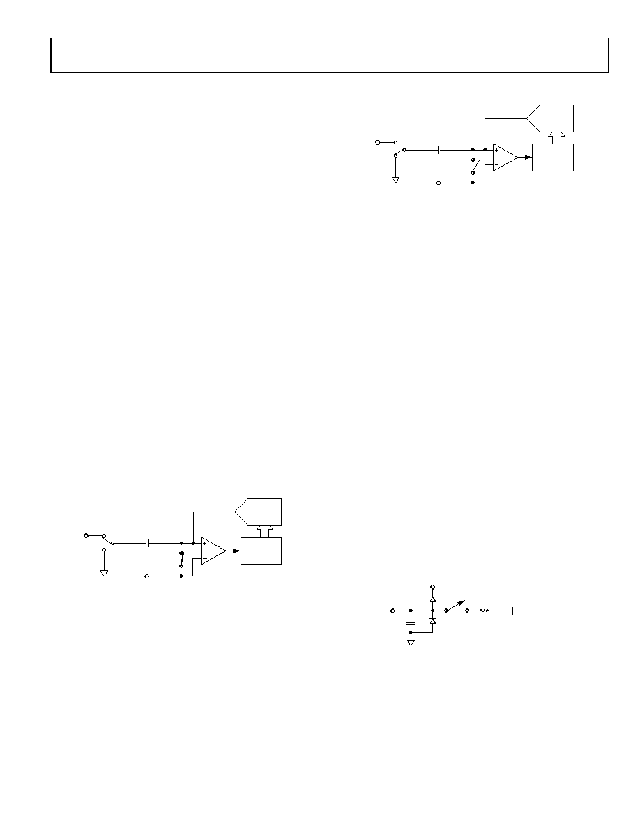
CONVERTER OPERATION
The AD7940 is a 14-bit, successive approximation ADC based
around a capacitive DAC. The AD7940 can convert analog
show simplified schematics of the ADC. The ADC comprises of
control logic, SAR, and a capacitive DAC. Figure 11 shows the
ADC during its acquisition phase. SW2 is closed and SW1 is in
Position A. The comparator is held in a balanced condition and
the sampling capacitor acquires the signal on the selected VIN
channel.
03305-0-004
CAPACITIVE
DAC
CONTROL
LOGIC
SAMPLING
CAPACITOR
COMPARATOR
ACQUISITION
PHASE
A
B
SW1
VDD/2
SW2
VIN
Figure 11. ADC Acquisition Phase
When the ADC starts a conversion, SW2 will open and SW1
will move to Position B, causing the comparator to become
unbalanced (Figure 12). The control logic and the capacitive
DAC are used to add and subtract fixed amounts of charge
from the sampling capacitor to bring the comparator back into
a balanced condition. When the comparator is rebalanced, the
conversion is complete. The control logic generates the ADC
output code (see the ADC Transfer Function section).
03305-0-005
CAPACITIVE
DAC
CONTROL
LOGIC
SAMPLING
CAPACITOR
COMPARATOR
CONVERSION
PHASE
A
B
SW1
VDD/2
SW2
VIN
Figure 12. ADC Conversion Phase
ANALOG INPUT
Figure 13 shows an equivalent circuit of the analog input
structure of the AD7940. The two diodes, D1 and D2, provide
ESD protection for the analog inputs. Care must be taken to
ensure that the analog input signal never exceeds the supply
rails by more than 300 mV. This will cause these diodes to
become forward-biased and to start conducting current into the
substrate. The maximum current these diodes can conduct
without causing irreversible damage to the part is 10 mA.
Capacitor C1 in Figure 13 is typically about 5 pF and primarily
can be attributed to pin capacitance. Resistor R1 is a lumped
component made up of the on resistance of a switch (track-and-
hold switch). This resistor is typically about 25 . Capacitor C2
is the ADC sampling capacitor and has a capacitance of 25 pF
typically. For ac applications, removing high frequency
components from the analog input signal is recommended by
use of an RC low-pass filter on the relevant analog input pin. In
applications where harmonic distortion and signal-to-noise
ratio are critical, the analog input should be driven from a low
impedance source. Large source impedances will significantly
affect the ac performance of the ADC. This may necessitate the
use of an input buffer amplifier. The choice of the op amp will
be a function of the particular application. When no amplifier is
used to drive the analog input, the source impedance should be
limited to low values. The maximum source impedance will
depend on the amount of total harmonic distortion (THD) that
can be tolerated. The THD will increase as the source impedance
increases, and performance will degrade (see Figure 8).
03305-0-006
R1
C2
30pF
CONVERSION PHASE - SWITCH OPEN
TRACK PHASE - SWITCH CLOSED
VIN
VDD
C1
4pF
D1
D2
Figure 13. Equivalent Analog Input Circuit
相关PDF资料 |
PDF描述 |
|---|---|
| AD7942BRMZ-RL7 | IC ADC 14BIT 250KSPS 10-MSOP |
| AD7944BCPZ | IC ADC 14BIT 2.5MSPS 20LFCSP |
| AD7946BCPZRL7 | IC ADC 14BIT 500KSPS 10-LFCSP |
| AD7948BN | IC DAC 12BIT MULT PARALL 20-DIP |
| AD7949BCPZRL7 | IC ADC 14BIT 250KSPS 8CH 20LFCSP |
相关代理商/技术参数 |
参数描述 |
|---|---|
| AD7940BRM-REEL7 | 功能描述:IC ADC 14BIT UNIPOLAR 8-MSOP RoHS:否 类别:集成电路 (IC) >> 数据采集 - 模数转换器 系列:- 标准包装:1,000 系列:- 位数:16 采样率(每秒):45k 数据接口:串行 转换器数目:2 功率耗散(最大):315mW 电压电源:模拟和数字 工作温度:0°C ~ 70°C 安装类型:表面贴装 封装/外壳:28-SOIC(0.295",7.50mm 宽) 供应商设备封装:28-SOIC W 包装:带卷 (TR) 输入数目和类型:2 个单端,单极 |
| AD7940BRMZ | 功能描述:IC ADC 14BIT UNIPOLAR 8-MSOP RoHS:是 类别:集成电路 (IC) >> 数据采集 - 模数转换器 系列:- 其它有关文件:TSA1204 View All Specifications 标准包装:1 系列:- 位数:12 采样率(每秒):20M 数据接口:并联 转换器数目:2 功率耗散(最大):155mW 电压电源:模拟和数字 工作温度:-40°C ~ 85°C 安装类型:表面贴装 封装/外壳:48-TQFP 供应商设备封装:48-TQFP(7x7) 包装:Digi-Reel® 输入数目和类型:4 个单端,单极;2 个差分,单极 产品目录页面:1156 (CN2011-ZH PDF) 其它名称:497-5435-6 |
| AD7940BRMZ-REEL7 | 功能描述:IC ADC 14BIT 100KSPS 8MSOP RoHS:是 类别:集成电路 (IC) >> 数据采集 - 模数转换器 系列:- 标准包装:1,000 系列:- 位数:16 采样率(每秒):45k 数据接口:串行 转换器数目:2 功率耗散(最大):315mW 电压电源:模拟和数字 工作温度:0°C ~ 70°C 安装类型:表面贴装 封装/外壳:28-SOIC(0.295",7.50mm 宽) 供应商设备封装:28-SOIC W 包装:带卷 (TR) 输入数目和类型:2 个单端,单极 |
| AD7940-DBRD | 功能描述:BOARD EVAL FOR AD7940 STAMP SPI RoHS:否 类别:编程器,开发系统 >> 评估板 - 模数转换器 (ADC) 系列:- 产品培训模块:Obsolescence Mitigation Program 标准包装:1 系列:- ADC 的数量:1 位数:12 采样率(每秒):94.4k 数据接口:USB 输入范围:±VREF/2 在以下条件下的电源(标准):- 工作温度:-40°C ~ 85°C 已用 IC / 零件:MAX11645 已供物品:板,软件 |
| AD7942 | 制造商:AD 制造商全称:Analog Devices 功能描述:16-Bit, +/-0.65 LSB INL, 500 kSPS PulSAR Differential ADC in MSOP/QFN |
发布紧急采购,3分钟左右您将得到回复。