参数资料
| 型号: | AD7945BRZ |
| 厂商: | Analog Devices Inc |
| 文件页数: | 7/16页 |
| 文件大小: | 0K |
| 描述: | IC DAC 12BIT MULTIPLYING 20-SOIC |
| 产品培训模块: | Data Converter Fundamentals DAC Architectures |
| 标准包装: | 37 |
| 设置时间: | 600ns |
| 位数: | 12 |
| 数据接口: | 并联 |
| 转换器数目: | 1 |
| 电压电源: | 单电源 |
| 功率耗散(最大): | 25µW |
| 工作温度: | -40°C ~ 85°C |
| 安装类型: | 表面贴装 |
| 封装/外壳: | 20-SOIC(0.295",7.50mm 宽) |
| 供应商设备封装: | 20-SOIC W |
| 包装: | 管件 |
| 输出数目和类型: | 1 电流,单极;1 电流,双极 |
| 采样率(每秒): | 1.7M |
| 产品目录页面: | 785 (CN2011-ZH PDF) |
AD7943/AD7945/AD7948
REV. B
–15–
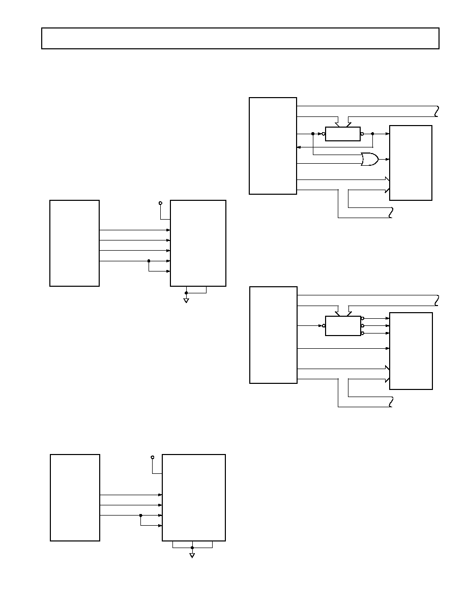
MICROPROCESSOR INTERFACING
AD7943 to ADSP-2101 Interface
Figure 17 shows the AD7943 to ADSP-2101 interface diagram.
The DSP is set up for alternate inverted framing with an inter-
nally generated SCLK. TFS from the ADSP-2101 drives the
STB1 input on the AD7943. The serial word length should be
set at 12. This is done by making SLEN = 11 (1011 binary).
The SLEN field is Bits 3–0 in the SPORT control register
(0x3FF6 for SPORT0 and 0x3FF2 for SPORT1).
With the 16 MHz version of the ADSP-2101, the maximum
output SCLK is 8 MHz. The AD7943 setup and hold time of
10 ns and 25 ns mean that it is compatible with the DSP when
running at this speed.
The OUTPUT FLAG drives both
LD1 and LD2 and is brought
low to update the DAC register and change the analog output.
ADSP-2101
AD7943
STB4
STB2
+5V
TFS
SCLK
DT
OUTPUT FLAG
CLR
STB3
LD1
LD2
STB1
SRI
Figure 17. AD7943 to ADSP-2101 Interface
AD7943 to DSP56001 Interface
Figure 18 shows the interface diagram for the AD7943 to the
DSP56001. The DSP56001 is configured for normal mode
synchronous operation with gated clock. The serial clock, SCK,
is set up as an output from the DSP and the serial word length
is set for 12 bits (WL0 = 1, WL1 = 0, in Control Register A).
SCK from the DSP56001 is applied to the AD7943
STB3 in-
put. Data from the DSP56000 is valid on the falling edge of
SCK and this is the edge which clocks the data into the AD7943
shift register. STB1, STB2 and STB4 are tied low on the
AD7943 to permanently enable the
STB3 input.
When the 12-bit serial word has been written to the AD7943,
the
LD1, LD2 inputs are brought low to update the DAC
register.
DSP56001
AD7943
STB4
STB2
STB1
+5V
SCK
STD
OUTPUT FLAG
CLR
STB3
LD1
LD2
SRI
Figure 18. AD7943 to DSP56001 Interface
AD7945 to MC68000 Interface
Figure 19 shows the MC68000 interface to the AD7945. The
appropriate data is written into the DAC in one MOVE instruc-
tion to the appropriate memory location.
MC68000
ADDRESS
DECODE
AD7945
CS
WR
DB11 – DB0
A1 – A23
AS
DTACK
R/
W
D15 – D0
Figure 19. AD7945 to MC68000 Interface
AD7948 to Z80 Interface
Figure 20 is the interface between the AD7948 and the 8-bit
bus of the Z80 processor. Three write operations are needed to
load the DAC. The first two load the MS byte and the LS byte
and the third brings the
LDAC low to update the output.
Z80
ADDRESS
DECODE
AD7948
CSMSB
WR
DB7 – DB0
A0 – A15
MREQ
WR
D7 – D0
CSLSB
LDAC
ADDRESS BUS
DATA BUS
Figure 20. AD7948 to Z80 Interface
相关PDF资料 |
PDF描述 |
|---|---|
| AD7945ARSZ-B | IC DAC 12BIT MULT PARALL 20SSOP |
| AD7945BRSZ | IC DAC 12BIT MULTIPLYING 20-SSOP |
| MS27473E24F4PA | CONN PLUG 56POS STRAIGHT W/PINS |
| MS27496E25F35P | CONN RCPT 128POS BOX MNT W/PINS |
| MS3108A36-9P | CONN PLUG 31POS RT ANG W/PINS |
相关代理商/技术参数 |
参数描述 |
|---|---|
| AD7945BRZ-AIRBUS | 制造商:Analog Devices 功能描述: |
| AD7945BRZ-REEL | 功能描述:IC DAC 12BIT MULT PARALL 20SOIC RoHS:是 类别:集成电路 (IC) >> 数据采集 - 数模转换器 系列:- 产品培训模块:LTC263x 12-, 10-, and 8-Bit VOUT DAC Family 特色产品:LTC2636 - Octal 12-/10-/8-Bit SPI VOUT DACs with 10ppm/°C Reference 标准包装:91 系列:- 设置时间:4µs 位数:10 数据接口:MICROWIRE?,串行,SPI? 转换器数目:8 电压电源:单电源 功率耗散(最大):2.7mW 工作温度:-40°C ~ 85°C 安装类型:表面贴装 封装/外壳:14-WFDFN 裸露焊盘 供应商设备封装:14-DFN-EP(4x3) 包装:管件 输出数目和类型:8 电压,单极 采样率(每秒):* |
| AD7945TQ | 制造商:Rochester Electronics LLC 功能描述:PARALLEL 12-B IOUT DAC IC - Bulk |
| AD7946 | 制造商:AD 制造商全称:Analog Devices 功能描述:14-Bit, 500 kSPS PulSAR⑩ ADC in MSOP/QFN |
| AD79461 | 制造商:AD 制造商全称:Analog Devices 功能描述:18-Bit, 2 MSPS PulSAR 15 mW ADC in LFCSP (QFN) |
发布紧急采购,3分钟左右您将得到回复。