- 您现在的位置:买卖IC网 > PDF目录10680 > AD7949BCPZ (Analog Devices Inc)IC ADC 14BIT 250KSPS 8CH 20LFCSP PDF资料下载
参数资料
| 型号: | AD7949BCPZ |
| 厂商: | Analog Devices Inc |
| 文件页数: | 32/32页 |
| 文件大小: | 0K |
| 描述: | IC ADC 14BIT 250KSPS 8CH 20LFCSP |
| 产品培训模块: | Power Line Monitoring |
| 产品变化通告: | Startup Circuitry Design Improvement Change 15/April/2009 |
| 标准包装: | 1 |
| 系列: | PulSAR® |
| 位数: | 14 |
| 采样率(每秒): | 250k |
| 数据接口: | DSP,MICROWIRE?,QSPI?,串行,SPI? |
| 转换器数目: | 1 |
| 功率耗散(最大): | 15.5mW |
| 电压电源: | 单电源 |
| 工作温度: | -40°C ~ 85°C |
| 安装类型: | 表面贴装 |
| 封装/外壳: | 20-VFQFN 裸露焊盘,CSP |
| 供应商设备封装: | 20-LFCSP-VQ |
| 包装: | 托盘 |
| 输入数目和类型: | * |
| 产品目录页面: | 780 (CN2011-ZH PDF) |
第1页第2页第3页第4页第5页第6页第7页第8页第9页第10页第11页第12页第13页第14页第15页第16页第17页第18页第19页第20页第21页第22页第23页第24页第25页第26页第27页第28页第29页第30页第31页当前第32页
Data Sheet
AD7949
Rev. D | Page 9 of 32
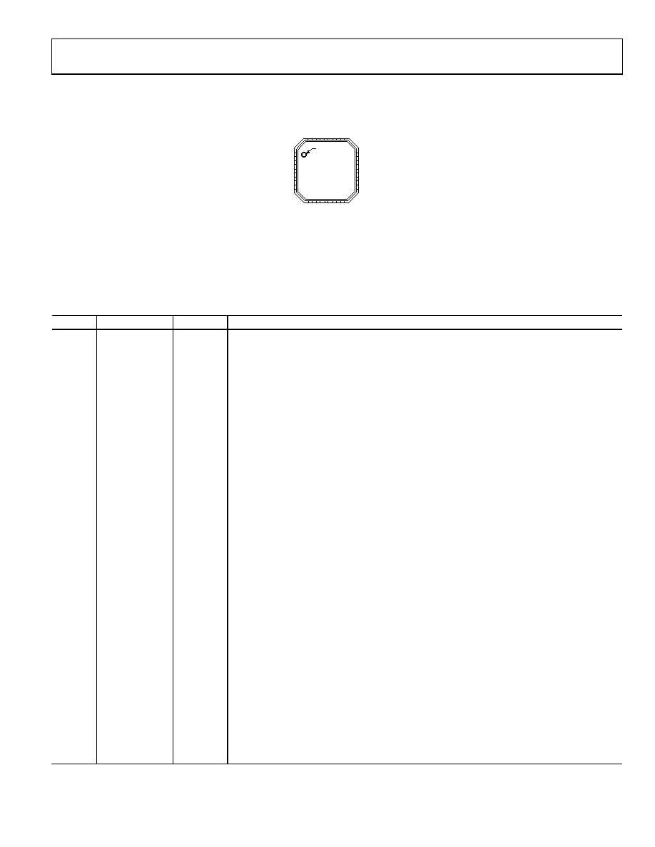
PIN CONFIGURATION AND FUNCTION DESCRIPTIONS
PIN 1
INDICATOR
1
VDD
2
REF
3
REFIN
4
GND
5
GND
13 SCK
14 SDO
15 VIO
12 DIN
11 CNV
6
IN4
7
IN5
8
IN6
0
1
CO
M
9
IN7
8
1
IN2
9
1
IN3
0
2
V
DD
7
1
IN1
6
1
IN0
TOP VIEW
(Not to Scale)
AD7949
NOTES
1. THE EXPOSED PAD IS NOT CONNECTED
INTERNALLY. FOR INCREASED
RELIABILITY OF THE SOLDER JOINTS, IT
IS RECOMMENDED THAT THE PAD BE
SOLDERED TO THE SYSTEM
GROUND PLANE.
07351-
004
Figure 4. Pin Configuration
Table 6. Pin Function Descriptions
Pin No.
Mnemonic
Type1
Description
1, 20
VDD
P
Power Supply. Nominally 2.5 V to 5.5 V when using an external reference and decoupled with
10 μF and 100 nF capacitors.
When using the internal reference for 2.5 V output, the minimum should be 3.0 V.
When using the internal reference for 4.096 V output, the minimum should be 4.5 V.
2
REF
AI/O
Reference Input/Output. See the Voltage Reference Output/Input section.
When the internal reference is enabled, this pin produces a selectable system reference = 2.5 V or
4.096 V.
When the internal reference is disabled and the buffer is enabled, REF produces a buffered
version of the voltage present on the REFIN pin (4.096 V maximum), useful when using low cost,
low power references.
For improved drift performance, connect a precision reference to REF (0.5 V to VDD).
For any reference method, this pin needs decoupling with an external 10 μF capacitor
connected as close to REF as possible. See the Reference Decoupling section.
3
REFIN
AI/O
Internal Reference Output/Reference Buffer Input. See the Voltage Reference Output/Input
section.
When using the internal reference, the internal unbuffered reference voltage is present and
needs decoupling with a 0.1 μF capacitor.
When using the internal reference buffer, apply a source between 0.5 V and 4.096 V that is
buffered to the REF pin as described above.
4, 5
GND
P
Power Supply Ground.
6 to 9
IN4 to IN7
AI
Channel 4 through Channel 7 Analog Inputs.
10
COM
AI
Common Channel Input. All input channels, IN[7:0], can be referenced to a common-mode
point of 0 V or VREF/2 V.
11
CNV
DI
Convert Input. On the rising edge, CNV initiates the conversion. During conversion, if CNV is
held high, the busy indictor is enabled.
12
DIN
DI
Data Input. This input is used for writing to the 14-bit configuration register. The configuration
register can be written to during and after conversion.
13
SCK
DI
Serial Data Clock Input. This input is used to clock out the data on SDO and clock in data on DIN
in an MSB first fashion.
14
SDO
DO
Serial Data Output. The conversion result is output on this pin, synchronized to SCK. In unipolar
modes, conversion results are straight binary; in bipolar modes, conversion results are twos
complement.
15
VIO
P
Input/Output Interface Digital Power. Nominally at the same supply as the host interface (1.8 V,
2.5 V, 3 V, or 5 V).
16 to 19
IN0 to IN3
AI
Channel 0 through Channel 3 Analog Inputs.
21
(EPAD)
Exposed Pad
(EPAD)
NC
The exposed pad is not connected internally. For increased reliability of the solder joints, it is
recommended that the pad be soldered to the system ground plane.
1
AI = analog input, AI/O = analog input/output, DI = digital input, DO = digital output, and P = power.
相关PDF资料 |
PDF描述 |
|---|---|
| 1676855-2 | CAP CER 0.56PF 100V 5% NP0 0603 |
| 1676855-1 | CAP CER 0.47PF 100V 5% NP0 0603 |
| 1676853-4 | CAP CER 0.82PF 25V 5% NP0 0603 |
| 1676853-3 | CAP CER 0.68PF 25V 5% NP0 0603 |
| VI-2NZ-MX-B1 | CONVERTER MOD DC/DC 2V 30W |
相关代理商/技术参数 |
参数描述 |
|---|---|
| AD7949BCPZ | 制造商:Analog Devices 功能描述:IC ADC 14BIT 250KSPS LFCSP-20 |
| AD7949BCPZRL7 | 功能描述:IC ADC 14BIT 250KSPS 8CH 20LFCSP RoHS:是 类别:集成电路 (IC) >> 数据采集 - 模数转换器 系列:PulSAR® 标准包装:1,000 系列:- 位数:16 采样率(每秒):45k 数据接口:串行 转换器数目:2 功率耗散(最大):315mW 电压电源:模拟和数字 工作温度:0°C ~ 70°C 安装类型:表面贴装 封装/外壳:28-SOIC(0.295",7.50mm 宽) 供应商设备封装:28-SOIC W 包装:带卷 (TR) 输入数目和类型:2 个单端,单极 |
| AD7949SCPZ-EP-R2 | 功能描述:14 Bit Analog to Digital Converter 8 Input 1 SAR 20-LFCSP-WQ (4x4) 制造商:analog devices inc. 系列:PulSAR? 包装:剪切带(CT) 零件状态:有效 位数:14 采样率(每秒):256k 输入数:8 输入类型:差分,单端 数据接口:SPI,DSP 配置:MUX-ADC 无线电 - S/H:ADC:- A/D 转换器数:1 架构:SAR 参考类型:外部, 内部 电压 - 电源,模拟:2.3 V ~ 5.5 V 电压 - 电源,数字:2.3 V ~ 5.5 V 特性:温度传感器 工作温度:-55°C ~ 125°C 封装/外壳:20-WFQFN 裸露焊盘,CSP 供应商器件封装:20-LFCSP-WQ(4x4) 标准包装:1 |
| AD7949SCPZ-EP-RL7 | 制造商:Analog Devices 功能描述:ADC Single SAR 250ksps 14-bit Serial 20-Pin LFCSP EP T/R 制造商:Analog Devices 功能描述:8 CH 250KSPS 14BIT ADC IC - Tape and Reel 制造商:Analog Devices 功能描述:IC ADC 14BIT 8CH 250KSPS 20LFCSP 制造商:Analog Devices 功能描述:Analog to Digital Converters - ADC 14-Bit 8CH 250 kSPS 制造商:Analog Devices 功能描述:CONVERTER - ADC |
| AD795 | 制造商:AD 制造商全称:Analog Devices 功能描述:Low Power, Low Noise Precision FET Op Amp |
发布紧急采购,3分钟左右您将得到回复。