- 您现在的位置:买卖IC网 > PDF目录10535 > AD7951BCPZ (Analog Devices Inc)IC ADC 14BIT 1MSPS 48-LFCSP PDF资料下载
参数资料
| 型号: | AD7951BCPZ |
| 厂商: | Analog Devices Inc |
| 文件页数: | 3/32页 |
| 文件大小: | 0K |
| 描述: | IC ADC 14BIT 1MSPS 48-LFCSP |
| 标准包装: | 1 |
| 系列: | PulSAR® |
| 位数: | 14 |
| 采样率(每秒): | 1M |
| 数据接口: | 串行,并联 |
| 转换器数目: | 1 |
| 功率耗散(最大): | 260mW |
| 电压电源: | 模拟和数字,双 ± |
| 工作温度: | -40°C ~ 85°C |
| 安装类型: | 表面贴装 |
| 封装/外壳: | 48-VFQFN 裸露焊盘,CSP |
| 供应商设备封装: | 48-LFCSP-VQ(7x7) |
| 包装: | 托盘 |
| 输入数目和类型: | 1 个差分,双极 |
第1页第2页当前第3页第4页第5页第6页第7页第8页第9页第10页第11页第12页第13页第14页第15页第16页第17页第18页第19页第20页第21页第22页第23页第24页第25页第26页第27页第28页第29页第30页第31页第32页
Data Sheet
AD7951
Rev. A | Page 11 of 32
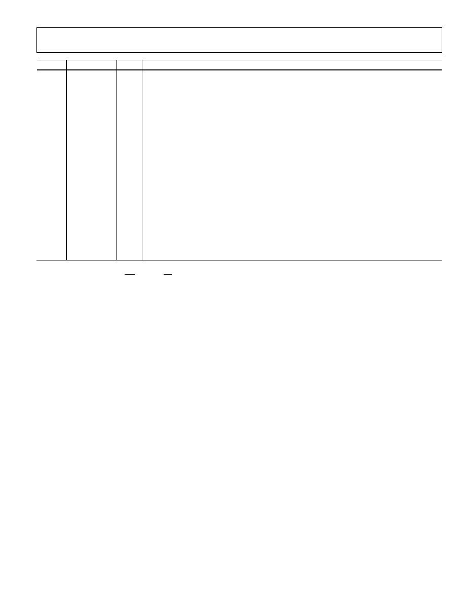
Pin No.
Mnemonic
Type1
Description
37
REF
AI/O
Reference Input/Output. When PDREF/PDBUF = low, the internal reference and buffer are enabled,
producing 5 V on this pin. When PDREF/PDBUF = high, the internal reference and buffer are disabled,
allowing an externally supplied voltage reference up to AVDD volts. Decoupling with at least a 22 μF is
required with or without the internal reference and buffer. See the Reference Decoupling section.
38
REFGND
AI
Reference Input Analog Ground. Connected to analog ground plane.
39
IN
AI
Analog Input Ground Sense. Should be connected to the analog ground plane or to a remote sense ground.
40
VCC
P
High Voltage Positive Supply. Normally +7 V to +15 V.
41
VEE
P
High Voltage Negative Supply. Normally 0 V to 15 V (0 V in unipolar ranges).
43
IN+
AI
Analog Input. Referenced to IN.
45
TEMP
AO
Temperature Sensor Analog Output. Enabled when the internal reference is turned on
(PDREF = PDBUF = low). See the Temperature Sensor section.
46
REFBUFIN
AI
Reference Buffer Input. When using an external reference with the internal reference buffer
(PDBUF = low, PDREF = high), applying 2.5 V on this pin produces 5 V on the REF pin.
See the Voltage Reference Input section.
47
PDREF
DI
Internal Reference Power-Down Input.
When low, the internal reference is enabled.
When high, the internal reference is powered down, and an external reference must be used.
48
PDBUF
DI
Internal Reference Buffer Power-Down Input.
When low, the buffer is enabled (must be low when using internal reference).
When high, the buffer is powered-down.
49
EPAD3
NC
Exposed Pad. The exposed pad is not connected internally. It is recommended that the pad be
soldered to VEE.
1 AI = analog input; AI/O = bidirectional analog; AO = analog output; DI = digital input; DI/O = bidirectional digital; DO = digital output; P = power.
2 In serial configuration mode (SER/PAR = high, HW/SW = low), this input is programmed with the serial configuration register and this pin is a don’t care. See the
3 LFCSP_VQ package only.
相关PDF资料 |
PDF描述 |
|---|---|
| VI-BTF-IV-F2 | CONVERTER MOD DC/DC 72V 150W |
| AD7951BSTZ | IC ADC 14BIT 1MSPS 48-LQFP |
| VI-B4P-MX-F1 | CONVERTER MOD DC/DC 13.8V 75W |
| VI-BTF-IV-F1 | CONVERTER MOD DC/DC 72V 150W |
| VI-BT4-IV-F4 | CONVERTER MOD DC/DC 48V 150W |
相关代理商/技术参数 |
参数描述 |
|---|---|
| AD7951BCPZRL | 功能描述:IC ADC 14BIT 1MSPS 48-LFCSP RoHS:是 类别:集成电路 (IC) >> 数据采集 - 模数转换器 系列:PulSAR® 标准包装:1,000 系列:- 位数:12 采样率(每秒):300k 数据接口:并联 转换器数目:1 功率耗散(最大):75mW 电压电源:单电源 工作温度:0°C ~ 70°C 安装类型:表面贴装 封装/外壳:24-SOIC(0.295",7.50mm 宽) 供应商设备封装:24-SOIC 包装:带卷 (TR) 输入数目和类型:1 个单端,单极;1 个单端,双极 |
| AD7951BSTZ | 功能描述:IC ADC 14BIT 1MSPS 48-LQFP RoHS:是 类别:集成电路 (IC) >> 数据采集 - 模数转换器 系列:PulSAR® 其它有关文件:TSA1204 View All Specifications 标准包装:1 系列:- 位数:12 采样率(每秒):20M 数据接口:并联 转换器数目:2 功率耗散(最大):155mW 电压电源:模拟和数字 工作温度:-40°C ~ 85°C 安装类型:表面贴装 封装/外壳:48-TQFP 供应商设备封装:48-TQFP(7x7) 包装:Digi-Reel® 输入数目和类型:4 个单端,单极;2 个差分,单极 产品目录页面:1156 (CN2011-ZH PDF) 其它名称:497-5435-6 |
| AD7951BSTZRL | 功能描述:IC ADC 14BIT 1MSPS 48-LQFP RoHS:是 类别:集成电路 (IC) >> 数据采集 - 模数转换器 系列:PulSAR® 标准包装:1,000 系列:- 位数:12 采样率(每秒):300k 数据接口:并联 转换器数目:1 功率耗散(最大):75mW 电压电源:单电源 工作温度:0°C ~ 70°C 安装类型:表面贴装 封装/外壳:24-SOIC(0.295",7.50mm 宽) 供应商设备封装:24-SOIC 包装:带卷 (TR) 输入数目和类型:1 个单端,单极;1 个单端,双极 |
| AD7952 | 制造商:AD 制造商全称:Analog Devices 功能描述:14-Bit, 1 MSPS, Differential, Programmable Input PulSAR ADC |
| AD7952BCPZ | 功能描述:IC ADC 14BIT DIFF 1MSPS 48LFCSP RoHS:是 类别:集成电路 (IC) >> 数据采集 - 模数转换器 系列:PulSAR® 标准包装:1,000 系列:- 位数:12 采样率(每秒):300k 数据接口:并联 转换器数目:1 功率耗散(最大):75mW 电压电源:单电源 工作温度:0°C ~ 70°C 安装类型:表面贴装 封装/外壳:24-SOIC(0.295",7.50mm 宽) 供应商设备封装:24-SOIC 包装:带卷 (TR) 输入数目和类型:1 个单端,单极;1 个单端,双极 |
发布紧急采购,3分钟左右您将得到回复。