- 您现在的位置:买卖IC网 > PDF目录10535 > AD7952BSTZ (Analog Devices Inc)IC ADC 14BIT DIFF 1MSPS 48-LQFP PDF资料下载
参数资料
| 型号: | AD7952BSTZ |
| 厂商: | Analog Devices Inc |
| 文件页数: | 1/32页 |
| 文件大小: | 0K |
| 描述: | IC ADC 14BIT DIFF 1MSPS 48-LQFP |
| 标准包装: | 1 |
| 系列: | PulSAR® |
| 位数: | 14 |
| 采样率(每秒): | 1M |
| 数据接口: | 并联 |
| 转换器数目: | 1 |
| 功率耗散(最大): | 260mW |
| 电压电源: | 模拟和数字,双 ± |
| 工作温度: | -40°C ~ 85°C |
| 安装类型: | 表面贴装 |
| 封装/外壳: | 48-LQFP |
| 供应商设备封装: | 48-LQFP(7x7) |
| 包装: | 托盘 |
| 输入数目和类型: | 1 个差分,双极 |
当前第1页第2页第3页第4页第5页第6页第7页第8页第9页第10页第11页第12页第13页第14页第15页第16页第17页第18页第19页第20页第21页第22页第23页第24页第25页第26页第27页第28页第29页第30页第31页第32页
14-Bit, 1 MSPS, Differential,
Programmable Input PulSAR ADC
Data Sheet
Rev. A
Information furnished by Analog Devices is believed to be accurate and reliable. However, no
responsibilityis assumedbyAnalogDevicesforitsuse,norforanyinfringementsof patentsorother
rightsofthirdpartiesthatmayresultfromitsuse.Specificationssubjecttochangewithoutnotice.No
license is granted by implication or otherwise under any patent or patent rights of Analog Devices.
Trademarksandregisteredtrademarksarethepropertyoftheirrespectiveowners.
One Technology Way, P.O. Box 9106, Norwood, MA 02062-9106, U.S.A.
Tel: 781.329.4700
2007–2012 Analog Devices, Inc. All rights reserved.
FEATURES
Multiple pins/software-programmable input ranges
+5 V (10 V p-p), +10 V (20 V p-p), ±5 V (20 V p-p),
±10 V (40 V p-p)
Pins or serial SPI-compatible input ranges/mode selection
Throughput
1 MSPS (warp mode)
800 kSPS (normal mode)
670 kSPS (impulse mode)
14-bit resolution with no missing codes
INL: ±0.3 LSB typical, ±1 LSB maximum (±61 ppm of FSR)
SNR: 85 dB @ 2 kHz
iCMOS process technology
5 V internal reference: typical drift 3 ppm/°C; TEMP output
No pipeline delay (SAR architecture)
Parallel (14- or 8-bit bus) and serial 5 V/3.3 V interface
SPI-/QSPI-/MICROWIRE-/DSP-compatible
Power dissipation
235 mW @ 1 MSPS
10 mW @ 1 kSPS
48-lead LQFP and 48-lead LFCSP (7 mm × 7 mm)
APPLICATIONS
Process controls
Medical instruments
High speed data acquisition
Digital signal processing
Instrumentation
Spectrum analysis
ATE
GENERAL DESCRIPTION
The AD7952 is a 14-bit, charge redistribution, successive
approximation register (SAR) architecture analog-to-digital
converter (ADC) fabricated on Analog Devices, Inc.’s iCMOS
high voltage process. The device is configured through hardware or
via a dedicated write-only serial configuration port for input
range and operating mode. The AD7952 contains a high speed
14-bit sampling ADC, an internal conversion clock, an internal
reference (and buffer), error correction circuits, and both serial
and parallel system interface ports. A falling edge on CNVST
samples the fully differential analog inputs on IN+ and IN.
The AD7952 features four different analog input ranges and three
different sampling modes: warp mode for the fastest throughput,
normal mode for the fastest asynchronous throughput, and
impulse mode where power is scaled with throughput.
Operation is specified from 40°C to +85°C.
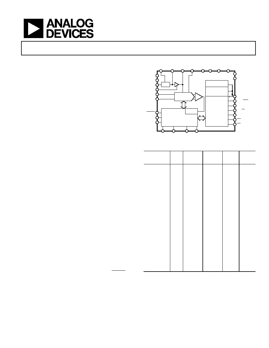
FUNCTIONAL BLOCK DIAGRAM
14
CONTROL LOGIC AND
CALIBRATION CIRCUITRY
CLOCK
AD7952
DGND
DVDD
AVDD
AGND
REF REFGND
IN+
PD
RESET
CNVST
PDBUF
REFBUFIN
PDREF
REF
TEMP
D[13:0]
BUSY
RD
CS
OB/2C
OGND
OVDD
BYTESWAP
SER/PAR
REF
AMP
SERIAL DATA
PORT
PARALLEL
INTERFACE
SWITCHED
CAP DAC
VCC VEE
WARP IMPULSE BIPOLAR TEN
SERIAL
CONFIGURATION
PORT
IN–
0
658
9-
0
01
Figure 1.
Table 1. 48-Lead PulSAR Selection
Input Type
Res
(Bits)
100 to
250
(kSPS)
500 to
570
(kSPS)
570 to
1000
(kSPS)
>1000
kSPS
Bipolar
14
Differential
Bipolar
14
AD7952
Unipolar
16
Bipolar
16
Differential
16
Unipolar
Simultaneous/
16
Multichannel
Unipolar
Differential
18
Unipolar
Differential
Bipolar
18
相关PDF资料 |
PDF描述 |
|---|---|
| DS34C87TM/NOPB | IC LINE DRIVER QUAD CMOS 16-SOIC |
| AD7951BCPZ | IC ADC 14BIT 1MSPS 48-LFCSP |
| VI-BTF-IV-F2 | CONVERTER MOD DC/DC 72V 150W |
| AD7951BSTZ | IC ADC 14BIT 1MSPS 48-LQFP |
| VI-B4P-MX-F1 | CONVERTER MOD DC/DC 13.8V 75W |
相关代理商/技术参数 |
参数描述 |
|---|---|
| AD7952BSTZRL | 功能描述:IC ADC 14BIT DIFF 1MSPS 48-LQFP RoHS:是 类别:集成电路 (IC) >> 数据采集 - 模数转换器 系列:PulSAR® 标准包装:1,000 系列:- 位数:12 采样率(每秒):300k 数据接口:并联 转换器数目:1 功率耗散(最大):75mW 电压电源:单电源 工作温度:0°C ~ 70°C 安装类型:表面贴装 封装/外壳:24-SOIC(0.295",7.50mm 宽) 供应商设备封装:24-SOIC 包装:带卷 (TR) 输入数目和类型:1 个单端,单极;1 个单端,双极 |
| AD795AH | 制造商:未知厂家 制造商全称:未知厂家 功能描述:Voltage-Feedback Operational Amplifier |
| AD795BH | 制造商:未知厂家 制造商全称:未知厂家 功能描述:Voltage-Feedback Operational Amplifier |
| AD795JN | 制造商:Analog Devices 功能描述:Operational Amplifier, Single AMP, Bipolar/JFET, 8 Pin, Plastic, DIP |
| AD795JR | 功能描述:IC OPAMP JFET 1.6MHZ LN 8SOIC RoHS:否 类别:集成电路 (IC) >> Linear - Amplifiers - Instrumentation 系列:- 标准包装:2,500 系列:Excalibur™ 放大器类型:J-FET 电路数:1 输出类型:- 转换速率:45 V/µs 增益带宽积:10MHz -3db带宽:- 电流 - 输入偏压:20pA 电压 - 输入偏移:490µV 电流 - 电源:1.7mA 电流 - 输出 / 通道:48mA 电压 - 电源,单路/双路(±):4.5 V ~ 38 V,±2.25 V ~ 19 V 工作温度:-40°C ~ 85°C 安装类型:表面贴装 封装/外壳:8-SOIC(0.154",3.90mm 宽) 供应商设备封装:8-SOIC 包装:带卷 (TR) |
发布紧急采购,3分钟左右您将得到回复。